User's Manual
|
|
| Rabbit 4000 Microprocessor User's Manual |
|
5. Memory Management
5.1 Overview
The Rabbit 4000 supports both 8-bit and 16-bit external flash and SRAM devices; three chip selects and two read/write-enable strobes allow up to six external devices to be attached at once. The 8-bit mode allows 0, 1, 2, or 4 wait states to be specified for each device, and the 16-bit mode allows 0 to 9 wait states depending on the settings. Both 8-bit and 16-bit page-mode devices are also supported.
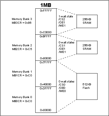
The Rabbit 4000's physical memory space contains four consecutive banks, each of which can be mapped to an individual chip-select/enable strobe pair. The banks can be set for equal sizes ranging from 128KB up to 4MB, providing a total physical memory range from 512KB up to 16MB. Figure 5-1 shows a sample configuration.
Either of the two most significant address bits (which are used to select the quadrant) can be inverted, providing the ability to bank-switch other pages from a larger memory device into the same memory bank.
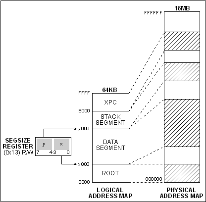
Code is executed in the 64KB logical memory space, which is divided into four segments: root, data, stack, and XMEM. The root segment is mapped directly to physical address 0x000000, while the data and stack segments can be mapped to 4KB boundaries anywhere in the physical space. The boundaries between the root and data segments and the data and stack segments can be adjusted in 4KB blocks as well.
The XMEM segment is a fixed 8KB and points to a physical memory address specified in the XPC register. It is possible to run code in the XMEM window, providing an easy means of storing and executing code beyond the 64KB logical memory space. Special call and return instructions to physical addresses are provided that automatically update the XPC register as necessary.
The Rabbit 2000 and 3000 had numerous instructions for reading and writing data to logical addresses, but only limited support for reading and writing data to a physical memory address. This has changed for the Rabbit 4000—a wide range of instructions has been provided to read and write to physical addresses. It is possible to use the same instructions to write to logical addresses as well.
The 64KB logical memory space limitation can also be expanded by using the separate instruction and data space mode. When this mode is enabled, address bit A16 is inverted for all data accesses in the root and/or data segments, while address bit A19 is inverted for all data accesses in the root and/or data segments before bank selection (physical device) occurs. These two features allow both code and data to access separate 64KB logical spaces instead of sharing a single space.
It is possible to protect memory in the Rabbit 4000 at three different levels: each of the memory banks can be made read-only, physical memory can be write-protected in 64KB blocks, and two of those 64KB blocks can be protected with a granularity of 4KB. A Priority 3 interrupt will occur if a write is attempted in one of the protected 64KB or 4KB blocks. In addition, it is possible to place limits around the code execution stack and generate an interrupt if a stack-related write occurs within 16 bytes of those limits.
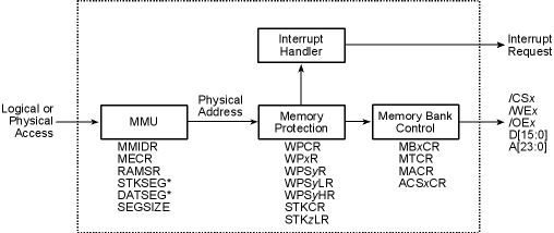
5.1.1 Block Diagram
5.1.2 Registers
5.2 Dependencies
5.2.1 I/O Pins
There are three chip select pins: /CS0, /CS1, and /CS2; two read strobes, /OE0 and /OE1; and two write strobes, /WE0 and /WE1.
There are eight dedicated data bus pins, D0 through D7. If the 16-bit mode is enabled, then PD0–PD7 automatically act as the upper byte of the data bus, D8 through D15.
There are 20 dedicated address pins, A0 through A19. Up to four more address pins can be enabled on PE0–PE3, representing A20 through A23.
Pin PE4 can be enabled as /A0 to allow byte reads and writes in 16-bit SRAM devices.
5.2.2 Clocks
All memory operations are clocked by the processor clock.
5.2.3 Other Registers
PEFR, PEALR
Enable A20-A23 and /A0.
5.2.4 Interrupts
When a write is attempted to a write-protected 64KB or 4KB block, a write-protection violation interrupt is generated. The interrupt request is cleared when it is handled. The write-protection violation interrupt vector is in the IIR at offset 0x090. It is always set to Priority 3.
When a stack-related write is attempted to a region outside that set by the stack limit registers, a stack limit violation occurs. The interrupt request is cleared when it is handled. The stack limit violation interrupt vector is in the IIR at offset 0x1B0. It is always set to Priority 3.
5.3 Operation
5.3.1 Memory Management Unit (MMU)
Code execution takes place in the 64KB logical memory space, which is divided into four segments: root, data, stack, and extended (XMEM). The root segment is always mapped starting at physical address 0x000000, but the other segments can be remapped to start at any physical 4KB block boundary.
The data and stack segment mappings are set by writing to the appropriate register, as shown in Table 5-1. The DATASEG and STACKSEG registers provide backwards compatibility to the Rabbit 2000 and 3000 processors; these registers map directly to DATASEGL and STACKSEGL but the corresponding uppermost four bits are set to zero.
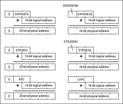
Each of these registers provides a 4KB offset that is added to the logical address to provide a physical address as shown in Figure 5-3.
5.3.2 8-bit Operation
On startup Memory Bank 0 is enabled to use /CS0, /OE0, and /WE0 with four wait states and write protection enabled; it is expected that an external flash device containing startup code be attached to those strobes. The other memory banks come up undefined and should be set via the appropriate MBxCR register to a valid setting before use.
The size of the memory banks can be defined in the MECR register. The default size is 256KB (the bank selection looks at address bits 18 and 19), but this value can be adjusted down to 128KB or up to 4MB per bank.
The two address bits used to select the bank can be inverted in MBxCR, which enables mapping different sections of a memory device larger than the current memory bank into memory. An example of this feature is shown in Figure 5-4.
It is possible to extend the timing of the /OE and/or /WE strobes by one half of a clock. This provides slightly longer strobes for slower memories; see the timing diagrams in Chapter 28. These options are available in MTCR.
It is possible to force /CS1 to be always active in MMIDR; enabling this will cause conflicts only if a device shares a /OE or /WE strobe with another device. This option allows faster access to particular memory devices.
5.3.3 16-bit and Page Modes
The Rabbit 4000 supports two additional memory modes to access both 16-bit and page-mode devices on /CS0 and /CS1, and can be enabled by writing to MACR. The first mode supports a 16-bit memory device in addition to the normal 8-bit memory devices. With this option, the memory device connected to /CS0 or /CS1 (or both) is assumed to have a 16-bit data path. Parallel Port D is used for the high byte of the data, and is configured automatically for this operation when a 16-bit mode is enabled, overriding any other Parallel Port D function.
Table 5-2. Advanced Memory Modes 8-bit
Basic 16-bit
Advanced
16-bit
Only instruction fetches from the 16-bit memory space actually read 16 bits. All data reads from the 16-bit memory space are eight bits, with the proper byte-lane swapping being done internally by the processor. In addition, because the processor can only handle a byte-wide stream of instructions, enabling the advanced 16-bit mode also enables an instruction prefetch queue. This queue is three bytes deep (in addition to the instruction register), but the prefetch mechanism only tries to keep it full with one byte. The other two bytes are for those cases where a prefetch was started in anticipation of the queue being emptied.
The prefetch mechanism tracks the instructions being fetched and executed to minimize bus conflicts between the prefetch mechanism and other bus transactions. These conflicts can occur if the execution (two clocks per byte minimum) is faster than the instruction prefetch (three clocks per two bytes minimum). The prefetch mechanism also attempts to minimize the impact of program branches. If a jump or subroutine call is decoded and the target address is being fetched the prefetch mechanism automatically stops prefetching once all of the target address is in the queue, in anticipation of taking the program branch
One special case of the prefetch mechanism is the block instructions. Because these instructions are interruptible and may rewind the PC, the prefetch mechanism will always empty the queue and restart the prefetching when leaving the block sequence while these instructions are being used.
The 16-bit memory device connected to /CS0 or /CS1 may or may not support byte writes, so there is an option to select between these two cases. Flash devices with a 16-bit bus do not support byte writes, so any byte writes or unaligned word writes to the 16-bit memory space will be suppressed (i.e., the /WE will not be asserted) with this option. Any aligned word writes are recognized internally and are combined into just one write transaction on the external bus. Internally the two writes still occur. The RAM option for the 16-bit bus does not inhibit byte writes or unaligned word writes and replicates the byte data on both halves of the data bus in these cases. In this mode the A0 and /A0 signals must be used by the memory to enable the individual bytes.
Table 5-3. A0 and /A0 Signals for Various Transaction Types Word Read (prefetch only)
Word Write
Byte Read or Write — Even Address
Byte Read or Write — Odd Address
All of the power-saving modes in Chapter 26 can still be used with the 16-bit mode. Because it is anticipated that the 16-bit memory may be slower than the normal 8-bit memories, separate wait-state controls for the 16-bit bus are provided in separate registers (ACS0CR and ACS1CR).
The second advanced bus mode is the Page Mode. This mode also can be enabled for either /CS0 or /CS1, and can be used with either 8-bit or 16-bit memories connected to these chip selects. Page-mode memories provide for a faster access time if the requested data is in the same page as the previous data. In the Rabbit 4000 (and most memory devices) a page is 16 bytes. Thus, if an address is identical to the previous address except in the lower four bits, the access time is assumed to be faster. These wait-state options are also controlled in the ACS0CR and ACS1CR.
In Page Mode the chip select and /OE remain active from one page access to the next, and only the four least-significant bits of the address change to request the new data. This obviously interferes with a number of the power-saving modes and will take precedence over them for /CS0 or /CS1 accesses, as appropriate. The power-saving modes will still apply to the other chip select and output enable signals. The logic recognizes which /OE is being used with each chip select in the Page Mode.
As mentioned previously, the ACS0CR and ACS1CR registers each contain three settings to control the generation of wait states in the advanced bus modes. These settings are used in place of the wait-state setting in MBxCR when an advanced bus mode is enabled. When the 16-bit bus is enabled, from one to seven automatic wait states for memory read bus cycles can be enabled. This setting is also used for the first access when the Page Mode is enabled; a second setting selects the number of wait states for all subsequent reads in the Page Mode, allowing from zero to three automatic wait states for the same-page accesses in the Page Mode. The third setting selects from five to nine automatic wait states for memory-write bus cycles. The choices available for the advanced bus wait states are sufficient to allow interfacing to a variety of standard memories for any Rabbit 4000 speed grade.
When a 16-bit memory is connected to /CS0, the first few instructions must program the device to operate in 16-bit mode. This code is shown below. This code should be the first thing executed by your device. Because the processor is fetching bytes from a 16-bit memory device that is not connected to A0, only one-byte instructions can be used, and they must occur in pairs.
ORG      0000h
XOR      A         ; a <= 00000000
XOR      A
LD       H, A      ; h <= 00000000
LD       H, A
SCF
SCF
RLA                ; a <= 00000001
RLA                ; a <= 00000010
LD       B, A      ; b <= 00000010
LD       B, A
SCF
SCF
ADC      A, B      ; a <= 00000101
ADC      A, B      ; a <= 00000111
ADD      A, A      ; a <= 00001110
ADD      A, A      ; a <= 00011100
SCF
SCF
ADC      A, H      ; a <= 00011101
ADC      A, H
LD       L, A      ; l <= 00011101
LD       L, A
IOI                ; two IOIs same as one
IOI
LD       (HL), B   ; MACR <= 00000010
LD       (HL), B   ; dummy memory write (no /WE)
NOP                ; required delay to start
NOP                ; up the 16-bit bus
5.3.4 Separate Instruction and Data Space
To make better use of the 64KB of logical space, an option is provided to map code and data accesses in the same address space to separate devices. This is accomplished by enabling the inversion of A16 and the most-significant bit of the bank select bits for accesses in the root and data segments. Careful use of these features allows both code and data to separately use up to 64KB of logical memory.
The RAM segment register (RAMSR) provides a shortcut for updating code by accessing it as data. It provides a "window" that uses the instruction address decoding when read or written as data.
The Rabbit 4000 Designer's Handbook provides further details on the use of the separate instruction and data space feature.
5.3.5 Memory Protection
Memory blocks may be protected at three separate granularities, as shown in Table 5-4. Writes can be prevented to any memory bank by writing to MBxCR. Writes can be prevented and trapped at a resolution of 64KB by enabling protection for that block in the appropriate WPxR register. For further control, two of those 64KB blocks can be further subdivided into 4KB blocks by selecting them as the write protect segments A or B.
When a write is attempted to a block protected in WPxR, WPSxLR, or WPSxHR, a Priority 3 write-protect interrupt occurs. This feature is automatically enabled by writing to the block protection registers; to disable it, set all the write-protect block registers to zero.
Table 5-4. Memory Protection Options Memory Bank
MBxCR, MECR
Write-Protect Blocks
WPCR, WPxR
Write Protect Segment A/B
WPSxR, WPSxLR, WPSxHR
5.3.6 Stack Protection
The Rabbit 4000 provides stack overflow and underflow protection. Low and high logical address limits can be set in STKLLR and STKHLR; a Priority 3 stack-violation interrupt occurs when a stack-based write occurs within the 16 bytes below the upper limit or within the 16 bytes above the lower limit. Note that the writes will still occur even if they are within the 16 bytes surrounding the limits, but the interrupt can serve as a warning to the application that the stack is in danger of being over or underrun.
The stack checking can be enabled or disabled by writing to STKCR.
When stack protection is enabled and a DMA transfer is occurring, the stack protection interrupt will occur if the lower 16 bits of a DMA transfer's physical write address match the 16 bits of the stack protection's logical address limits.
5.4 Register Descriptions
The current contents of this register are reported.
Eight LSBs (MSBs are set to zero by write) of physical address offset to use if
SEGSIZ[7:4] ≤ Addr[15:12] < 0xE
The current contents of this register are reported.
Eight LSBs of physical address offset to use if SEGSIZ[7:4] ≤ Addr[15:12] < 0xE
The current contents of this register are reported.
Eight LSBs (MSBs are set to zero by write) of physical address offset to use if: SEGSIZ[3:0] ≤ Addr[15:12] < SEGSIZ[7:4]
Eight LSBs of physical address offset to use if: SEGSIZ[3:0] ≤ Addr[15:12] < SEGSIZ[7:4]
These bits are reserved and should always be written as zero. These bits always return zeros when read.
Four MSBs of physical address offset to use if:
SEGSIZ[3:0] <= Addr[15:12] < SEGSIZ[7:4]
The current contents of this register are reported.
Boundary value for switching from DATSEG to STKSEG for translation.
Boundary value for switching from none to DATSEG for translation.
These bits are reserved and should be written with zeros.
Write protection in User Mode only.
Write protection in System and User modes.
When these eight bits [23:16] match bits of the physical address, write-protect that 64K range in 4K increments using WPSxLR and WPSxHR.
These bits are reserved and should be written with zeros.
Disable stack-limit checking.
Enable stack-limit checking.
Lower limit for stack-limit checking. If a stack operation or stack-relative memory access is attempted at an address less than {STKLLR, 0x10}, a stack-limit violation interrupt is generated.
Upper limit for stack-limit checking. If a stack operation or stack-relative memory access is attempted at an address greater than {STKHLR, 0xEF}, a stack-limit violation interrupt is generated.
| Rabbit Semiconductor www.rabbit.com |