User's Manual
|
|
| Rabbit 4000 Microprocessor User's Manual |
|
28. Specifications
28.1 DC Characteristics
28.2 AC Characteristics
28.3 Memory Access Times
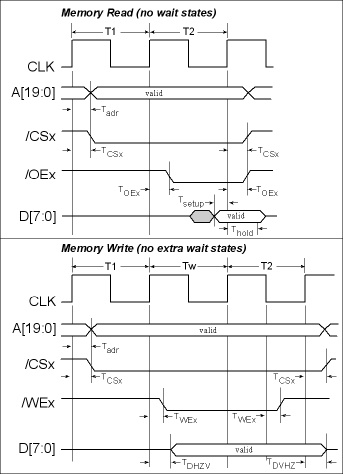
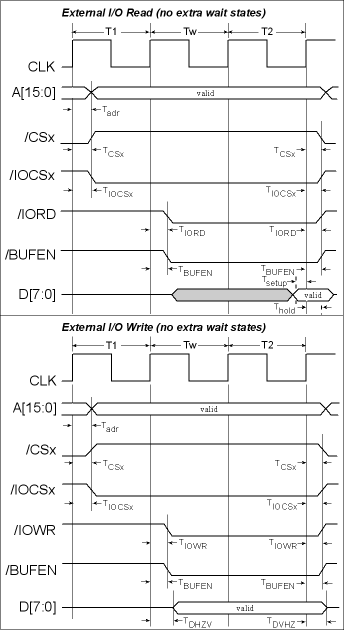
All access time measurements are taken at 50% of signal height.
28.3.1 Memory Reads
28.3.2 Memory Writes
28.3.3 External I/O Reads
28.3.4 External I/O Writes
NOTE /IOCSx can be programmed to be active low (default) or active high. 28.3.5 Memory Access Times
In computing memory requirements, the important considerations are the address access time, output-enable access time, and minimum write-pulse required. Increasing the clock doubler delay increases the output-enable time, but decreases the memory write-pulse width. The early write-pulse option can be used to ensure a long-enough write pulse, but then it must be ensured that the write pulse does not begin before the address lines have stabilized.
The clock doubler has an affect on the memory access times. It works by ORing the clock with a delayed version of itself. The nominal delay varies from 3 to 20 ns, and is set under program control. Any asymmetry in the main clock input before it is doubled will result in alternate clocks having slightly different periods. Using the suggested oscillator circuit, the asymmetry is no worse than 52%–48%. This results in a given clock being shortened by the ratio 50/52, or 4% worst-case. The memory access time is not normally affected because the memory bus cycle is two clocks long and includes both a long and a short clock, resulting in no net change arising from asymmetry. However, if an odd number of wait states is used, then the memory access time will be affected slightly.
When the clock spectrum spreader is enabled, clock periods are shortened by a small amount, depending on whether the "normal" or the "strong" spreader setting is used, and depending on the operating voltage. If the clock doubler is used, the spectrum spreader affects every other cycle and reduces the clock high time. If the doubler is not used, then the spreader affects every clock cycle, and the clock low time is reduced. Of course, the spectrum spreader also lengthens clock cycles, but only the worst-case shortening is relevant for calculating worst-case access times. The numbers given for clock shortening with the doubler disabled are the combined shortening for two consecutive clock cycles, worst case.
The required memory address and output-enable access time for some typical clock speeds are given in Table 28-8 below. It is assumed that the clock doubler is used, that the clock spreader is enabled in the normal mode, that the memory early output-enable is on, and that the address bus has a load of 60 pF.
Table 28-8. Preliminary Memory Requirements
(VDDCORE = 1.8 V ± 10%, VDDIO = 3.3 V ± 10%, TA = -40°C to 85°C,
address bus loading = 60 pF)
All important signals on the Rabbit 4000 are output-synchronized with the internal clock. The internal clock is closely synchronized with the external clock, which is available on the CLK pin. The delay in signal output depends on the capacitive load on the output lines. In the case of the address lines, which are critically important for establishing memory access time requirements, the capacitive loading is usually in the range of 25–100 pF, and the load is due to the input capacitance of the memory devices and PC trace capacitance.
Delays are expressed from the waveform midpoint in keeping with the convention used by memory manufacturers.
Table 28-9 lists the delays in gross memory access time for several values of VDDIO.
Table 28-9. Preliminary Data and Clock Delays
(VDD ±10%, Temp. -40°C to 85°C)
When the spectrum spreader is enabled with the clock doubler, every other clock cycle is shortened or lengthened by a maximum amount given in the table above. The shortening takes place by shortening the high part of the clock. If the doubler is not enabled, then every clock is shortened during the low part of the clock period. The maximum shortening for a pair of clocks combined is shown in the table.
The gross memory access time is 2T, where T is the clock period. To calculate the actual memory access time, subtract the clock to address output time, the data in setup time, and the clock period shortening due to the clock spectrum spreader from 2T.
Example Memory Access Time Calculation
access time = 2T - (clock to address) - (data setup) - (spreader delay)
- clock = 29.49 MHz, so T = 34 ns
- operating voltage is 3.3 V
- bus loading is 60 pF
- clock to address output delay = 8 ns (see Table 28-9)
- data setup time = 1 ns
- spectrum spreader is on in 1 ns mode, resulting in a loss of 3 ns worst-case (see Table 28-9)
= 68 ns - 8 ns - 1 ns - 3 ns
= 56 ns
Similarly, the gross output-enable access time is T + minimum clock low time (it is assumed that the early output enable option is enabled). This is reduced by the spectrum spreader loss, the time from clock to output for the output enable signal, the data setup time, and a correction for the asymmetry of the original oscillator clock.
Example Output-Enable Access Time Calculation
- clock = 29.49 MHz, so T = 34 ns
- operating voltage is 3.3 V
- the clock doubler has a nominal delay of 16 ns (see Table 28-8), resulting in a minimum clock low time of 80% × 16 ns = 12.8 ns
- clock to output enable is 5 ns (assuming 20 pF load)
- spectrum spreader is on in 1 ns mode, resulting in a loss of 4.5 ns worst-case (see Table 28-9)
- main clock asymmetry is 52% / 48%, resulting in a loss of 4% of the clock period, or 1.4 ns
The output enable access time is given by
access time = T + (min. clock low) - (clock to output enable) -
(spreader delay) - (asymmetry delay) - (data setup time)
= 34 ns + 12.8 ns - 5 ns - 4.5 ns - 1.4 ns
= 36 ns
28.4 Clock Speeds
28.4.1 Recommended Clock/Memory Configurations
The preferred configuration for a Rabbit-based system is to use an external crystal or resonator that has a frequency one-half of the maximum internal clock frequency. The oscillator frequency can be doubled or divided by 2, 4, 6, or 8, giving a variety of operating speeds from the same crystal frequency. In addition, the 32.768 kHz oscillator that drives the battery-backable clock can be used as the main processor clock and, to save the substantial power consumed by the fast oscillator, the fast oscillator can be turned off. This scenario is called the sleepy mode, where the clock speed is from 2 kHz to 32 kHz, and the operating system current consumption of 10 to 120 µA depends on frequency and voltage.
Table 28-10 describes some recommended clock and memory configurations for both 8-bit and 16-bit memory devices. Optimal configurations for using 15 ns, 45–55 ns, and 70 ns memories are shown. Note that there is always at least one wait state in the 16-bit mode.
The Rabbit 4000 is rated for a minimum clock period of 16 ns for both commercial and industrial specifications (preliminary). The commercial rating calls for a ±5% voltage variation from 3.3 V, and a temperature range from -40 to + 70°C. The industrial ratings stretch the voltage variation to ±10% over a temperature range from -40 to + 85°C. This corresponds to maximum clock frequencies of about 60 MHz (commercial or industrial). If the clock doubler or spectrum spreader is used, these maximum ratings must be reduced as shown in Table 28-11.
When the doubler is used, the duty cycle of the clock becomes a critical parameter. The duty cycle should be measured at the separate clock output pin (pin 2). The minimum period must be increased by any amount that the clock high time is greater or less than specified in the duty-cycle requirement.
For example, consider a design where the spreader and doubler are enabled, with 8 ns nominal delay in the doubler. The high and low clock are equal to within 1 ns. This violates the duty cycle requirement by 3 ns since (clock low - clock high) can be as small as -1 ns, but the requirement is that it not be less than 2 ns. Thus, 3 ns must be added to the minimum period of 21 ns, giving a minimum period of 24 ns and a maximum frequency of 41.6 MHz (commercial).
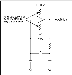
Since the built-in high-speed oscillator buffer generates a clock that is very close to having a 50% duty cycle, to obtain the highest clock speeds using the clock doubler you must use an external oscillator buffer that will allow for duty-cycle adjustment by changing the resistance of the power and ground connections as shown below.
28.5 Power and Current Consumption
Various mechanisms contribute to the current consumption of the Rabbit 4000 processor while it is operating, including current that is proportional to the voltage alone (leakage current) and dependent on both voltage and frequency (switching and crossover current). To reduce current consumption, the clock can be divided down in one of the sleepy modes; see Table 26-1 for more details.
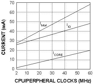
Figure 28-5 shows a typical current draw as a function of the main clock frequency. The values shown do not include any current consumed by external oscillators or memory. It is assumed that approximately 30 pF is connected to each address line.
28.5.1 Sleepy Mode Current Consumption
The Rabbit 4000 supports designs with very low power consumption by using features such as the ultra-sleepy modes and self-timed chip selects. At the low frequencies possible in the ultra-sleepy modes (as low as 2 kHz), the external memory devices become significant factors in the current consumption unless one of the short or self-timed chip selects are used.
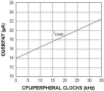
Figure 28-6 shows a typical current draw for the ultra sleepy modes.
28.5.2 Battery-Backed Clock Current Consumption
For the battery-backed features of the Rabbit 4000 to perform while the processor is powered down, both the VBAT and BATIO pins need to be supplied properly. The VBAT pin powers the internal real-time clock and the battery-backed SRAM, while VBATIO powers the /RESET, /CS1, CLK32K, and RESOUT pins.
Note that the VBATIO pin can be powered at 1.8 V during powerdown even if the processor is running at 3.3 V normally. A circuit to switch between a 1.8–2.0 V battery and the main power can use the RESOUT pin to switch the power source for the VBATIO pin. R is a current-limiting resistor that should be adjusted for the battery voltage; a good value to use for a 2.0 V battery is 150 kohms.
Table 28-12 shows the typical current consumption for these pins while the remainder of the Rabbit 4000 is powered down.
Table 28-12. Typical Battery-Backed Current Consumption
(-40°C to +85°C)
| Rabbit Semiconductor www.rabbit.com |