29. Package Specifications and Pinout
29.1 LQFP Package
29.1.1 Pinout
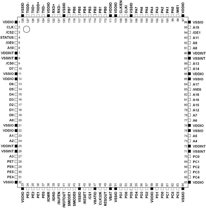
Figure 29-1. Package Outline and Pin Assignments
29.1.2 Mechanical Dimensions and Land Pattern

Figure 29-2. Mechanical Dimensions Rabbit LQFP Package
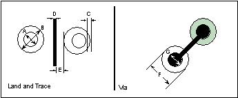
Figure 29-3 shows the PC board land pattern for the Rabbit 4000 chip in a 128-pin LQFP package. This land pattern is based on the IPC-SM-782 standard developed by the Surface Mount Land Patterns Committee and specified in Surface Mount Design and Land Pattern Standard, IPC, Northbrook, IL, 1999.
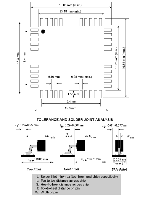
Figure 29-3. PC Board Land Pattern for Rabbit 4000 128-pin LQFP
29.2 Ball Grid Array Package
29.2.1 Pinout
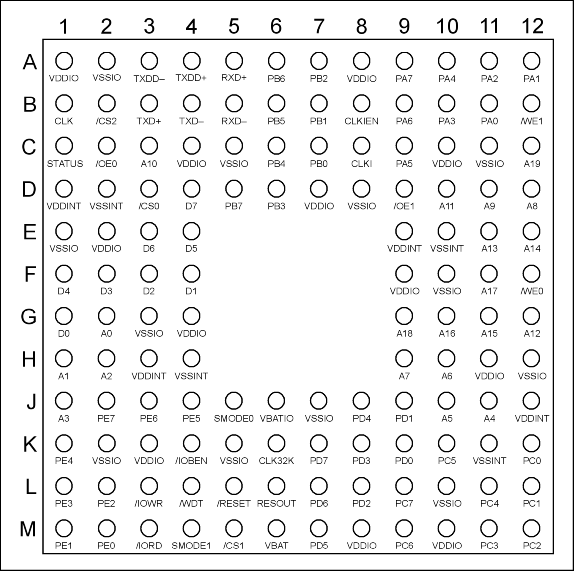
Figure 29-4. Ball Grid Array Pinout Looking Through the Top of Package
29.2.2 Mechanical Dimensions and Land Pattern
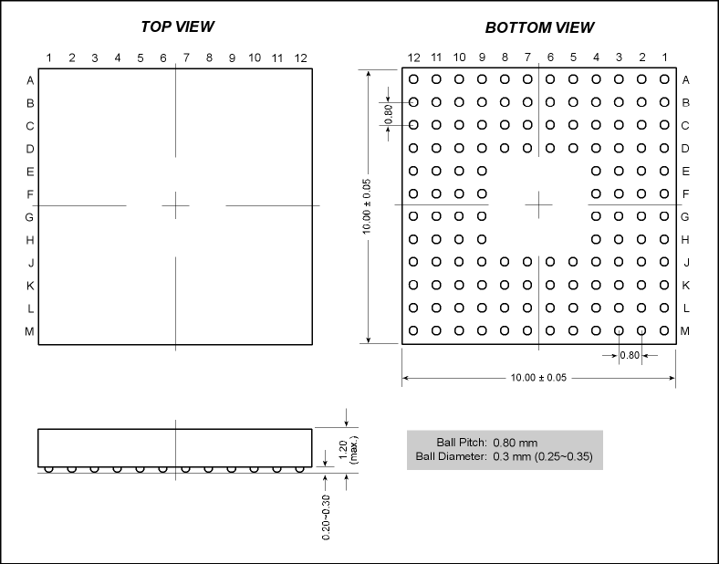
Figure 29-5. BGA Package Outline
Table 29-1. Ball and Land Size Dimensions
Nominal Ball Diameter
(mm) |
Tolerance Variation
(mm) |
Ball Pitch
(mm) |
Nominal Land Diameter
(mm) |
Land Variation (mm) |
|
|
|
|
|
|
The design considerations in Table 29-2 are based on 5 mil design rules and assume a single conductor between solder lands.
Table 29-2. Design Considerations
(all dimensions in mm)
|
|
|
Solder Land Diameter
|
|
|
|
NSMD Defined Land Diameter
|
|
|
|
Land to Mask Clearance (min.)
|
|
|
|
Conductor Width (max.)
|
|
|
|
Conductor Spacing (typ.)
|
|
|
|
Via Capture Pad (max.)
|
|
|
|
Via Drill Size (max.)
|
|
29.3 Rabbit Pin Descriptions
Table 29-3 lists all the pins on the Rabbit 4000 along with the data direction of the pin, its function, and the pin number on the die.
Table 29-3. Rabbit 4000 Pin Descriptions
|
Hardware
|
CLK
|
Output
|
Internal Clock Output
|
|
|
CLK32K
|
Input
|
32 kHz Clock In
|
|
|
/RESET
|
Input
|
Master Reset
|
|
|
RESOUT
|
Output
|
Reset Output
|
|
|
CLKI
|
Input
|
Main Clock In
|
|
|
CLKIEN
|
Output
|
Main Clock Enable
|
|
|
CPU Buses
|
A[19:0]
|
Output
|
Address Bus
|
|
|
D[7:0]
|
Bidirectional
|
Data Bus
|
|
|
Status &
Control
|
/WDTOUT
|
Output
|
Watchdog Timer Timeout
|
|
|
STATUS
|
Output
|
Instruction Fetch First Byte
|
|
|
SMODE1
SMODE0
|
Input
|
Bootstrap Mode & Tamper Detect
|
|
|
Chip Selects
|
/CS0
|
Output
|
Memory Chip Select 0
|
|
|
/CS1
|
Output
|
Memory Chip Select 1
|
|
|
/CS2
|
Output
|
Memory Chip Select 2
|
|
|
Output Enables
|
/OE0
|
Output
|
Memory Output Enable 0
|
|
|
/OE1
|
Output
|
Memory Output Enable 1
|
|
|
Write Enables
|
/WE0
|
Output
|
Memory Write Enable
|
|
|
/WE1
|
Output
|
Memory Write Enable
|
|
|
I/O Control
|
/BUFEN
|
Output
|
I/O Buffer Enable
|
|
|
/IORD
|
Output
|
I/O Read Enable
|
|
|
/IOWR
|
Output
|
I/O Write Enable
|
|
|
I/O Ports
|
PA[7:0]
|
Input/Output
|
I/O Parallel Port A
|
|
|
PB[7:0]
|
Input/Output
|
I/O Parallel Port B
|
|
|
PC[7:0]
|
Input/Output
|
I/O Parallel Port C
|
|
|
PD[7:0]
|
Input/Output
|
I/O Parallel Port D
|
|
|
PE[7:0]
|
Input/Output
|
I/O Parallel Port E
|
|
|
Network
|
TXD+
TXD-
TXDD+
TXDD-
|
Output
|
Network Transmit
|
|
|
RXD+
RXD-
|
Input
|
Network Receive
|
|
|
