User's Manual
|
|
| Rabbit 4000 Microprocessor User's Manual |
|
27. System/User Mode
27.1 Overview
The Rabbit 4000 provides support for two tiers of control in the processor: System Mode, which provides full access to all processor resources; and User Mode, a more restricted mode. Table 27-1 describes the essential differences between the System Mode and the User Mode. The System Mode is essentially the same as the normal operation when the System/User Mode is disabled.
The main intent of the System/User Mode is to protect critical code (for example, code that performs remote firmware updates), data, and the current processor state (memory setup, peripheral control, etc.) from inadvertent changes by the user's standard code. By removing access to the processor's I/O registers and preventing memory writes to critical regions, the user's code can run without the danger of locking up the processor to the point where it cannot be restarted remotely and/or new code uploaded.
27.1.1 Registers
27.2 Dependencies
27.2.1 I/O Pins
There are no pin dependencies for the System/User Mode.
27.2.2 Clocks
There are no clock dependencies for the System/User Mode.
27.2.3 Other Registers
Any writes to the internal I/O registers listed in Table 27-2 are ignored when the System/User Mode is enabled and the processor is in the User Mode.
27.2.4 Interrupts
The System Mode Violation interrupt occurs whenever the IDET instruction is executed while the System/User mode is enabled and the processor is in the User Mode. Its purpose is to trap when system code is being executed while the processor is in the User Mode.
The System Mode Violation interrupt vector is in the IIR at offset 0x180. It always occurs at Priority 3.
Note that Priority 3 is not available while the System/User Mode is enabled and the processor is in the User Mode. If the processor is placed into Priority 3 either by an instruction or an interrupt, it will respond as if it was set to Priority 2.
When the System/User Mode is enabled, it is critical to handle the SU stack in interrupts as well as the IP stack; always perform a
SURESbefore theIPRESat the end of the interrupt.27.3 Operation
The System/User Mode is designed to work with the memory and stack protection features of the Rabbit 4000 processor to provide a seamless framework for protection of critical code. However, there are many levels at which the System/User Mode can be used — some examples are described here.
27.3.1 Memory Protection Only
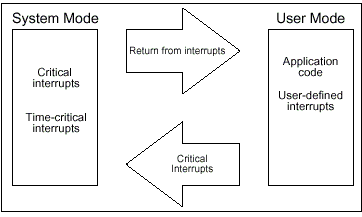
At the beginning of the user program, all necessary peripherals are enabled, all peripheral interrupts to be used are set up for the User Mode, critical memory regions are protected, stack limits are set, and the various system/memory/stack violation interrupts are enabled. The processor then enters the User Mode and remains in the User Mode for all operations (interrupts can be handled however the user desires). Obviously the critical interrupts can be handled in the System Mode, but at that point the device is typically reset and the error is logged. Figure 27-1 shows an overview of this level of operation.
27.3.2 Mixed System/User Mode Operation
This mode is similar to the previous mode, but with some portions of the program written for System Mode — for example, peripheral interrupts where latency is critical. By keeping the System Mode code sections small, potential system crashes are still minimized. Figure 27-2 shows an overview of this level of operation.
27.3.3 Complete Operating System
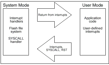
This section describes a "full" use of the System/User Mode — separating all common functions into a System Mode "operating system" while letting the application-specific code run in the User Mode. By default, the System Mode handles all peripherals and interrupts, as well as high-level interfaces such as a flash file system. However, the processor will be running the application code in the User Mode most of the time.
The application code can request direct access to a peripheral and/or interrupt from the System Mode. If allowed, the System Mode can create an interrupt vector as described in Section 27.3.7 that will execute the user code interrupt handler.
When the application code wants to perform an action that is controlled by the System Mode, it can request the particular action by loading the appropriate value into HL and executing SYSCALL. This requires generating a list of all the actions that the application code would want to do, assigning values to each action, and implementing a SYSCALL handler in the System Mode that parses the value passed to it and calls the appropriate function.
Write protection should be enabled (User Mode only) for all blocks containing system code and data as well as any critical memory regions.
If any critical interrupts occur (stack limit violation, system mode violation, write protection violation), System Mode handlers can perform any of a number of operations: restart the application code, signal another device, halt operation, and so on.
Figure 27-3 shows an overview of this level of operation.
27.3.4 Enabling the System/User Mode
The following steps describe how to enable the System/User Mode.
- If a peripheral needs to be accessed while in User Mode, write to the appropriate user enable register to allow that access.
- Write a 1 to bit 0 of EDMR to enable System/User Mode.
- Execute the SETUSR instruction to enter User Mode.
After the User Mode is entered, the limitations described earlier are in effect — writes to protected registers will be ignored, Priority 3 is not available, and executing an IDET will cause a System Mode Violation interrupt. Other features such as write protection may be effect for user mode as well.
27.3.5 System/User Mode Instructions
Seven instructions exist primarily to support the System/User Mode, and are listed in Table 27-3. Note that
IDETshares the value ofLD E,Ein the opcode table, and will always perform that operation (but will have special behavior when the System/User Mode is enabled and the processor is in System Mode). In addition, if the ALTD prefix appears before the instruction,LD E',Eis always executed and the special behavior does not occur.
The processor keeps a one-byte stack (called the SU register) that is analogous to the IP register that keeps track of the interrupt priority. Every time
SETUSRis executed (to enter the User Mode), or an interrupt occurs, orSYSCALLorRSTis executed (to enter System Mode), the current mode is pushed onto the SU register. When aSURESis executed, the previous mode is popped off the SU register.The effects of each instruction are:
- The
SETUSRinstruction puts the processor into the User Mode by pushing the correct value into the SU register.
PUSH SUandPOP SUpush and pop the single-byte SU register on/off the SP stack.
SURESpops the current processor mode off the SU register, returning it to the previous mode.
IDETcauses an interrupt if executed in the User Mode, and does nothing in System Mode. It is intended to be placed in system-level code and trap any execution of that code while in the User Mode.
RDMODEreturns the current mode in the carry flag (0 for System Mode, 1 for User Mode).
SYSCALLis essentially a newRSTinstruction, and was added to allow User Mode access to the System Mode without using one of the existingRSTinstructions. It will put the processor into the System Mode and execute code in the corresponding interrupt-vector table entry.
SCALLis anotherRSTinstruction that vectors to the same address asSYSCALL. The difference is that it also pushes the value of the SU register as well as the return address onto the stack.
SRETis the companion instruction toSCALL; it expects both SU and the return address to be on the stack.
SETSYSPandSETUSRPare support functions for handing user mode interrupts. pushes a 16-bit compare value onto the stack and enters user mode.SETSYSPpops a 16-bit value off the stack and compares it to the provided value; a system mode violation interrupt occurs if they do not match. These two instructions provide protection for User Mode interrupts by checking for both main stack and SU stack mismatches when the User Mode handler returns.27.3.6 System Mode Violation Interrupt
The following steps describe how to set up the System Mode Violation interrupt.
- Write the vector to the interrupt service routine to the internal interrupt table.
- Enable the system/user mode by writing to EDMR.
- The interrupt request is cleared automatically when handled.
A sample interrupt handler is shown below.
sysmode_isr::
   push af
; handle the system mode violation here
   pop af
   sures
   ipres
   ret
27.3.7 Handling Interrupts in the System/User Mode
Interrupts,
RSTs,SYSCALL, andSCALLall enter the System Mode automatically. There will be times, however, that an interrupt should be handled in the User Mode. The solution to this is for System Mode interrupt vector to reenter the User Mode before calling the User Mode interrupt handler. An example of both system and user interrupt handling is shown in Figure 27-4.When enabled for User Mode access, a peripheral interrupt (if it is capable of generating an interrupt) can only be requested at Priority 2 or 1.
Some sample code for both System Mode interrupts and User Mode interrupts is shown below. The use of
SETUSRPandSETSYSPprovides checks against stack mismatches and incorrect System/User Modes coming out of the User Mode handler.
systemmode_isr:                ; jumped to from interrupt vector table
    ... handle interrupt ...
   sures                       ; reenter previous mode
   ipres                       ; restore previous interrupt priority
   ret
usermode_isr:                  ; jumped to from interrupt vector table
                               ;    (still in system mode at this point)
   push su                     ; preserve current SU stack
   setusrp 0x1234              ; enter user mode with stack compare value
   call user_handler           ; handle interrupt at user level
   setsysp 0x1234              ; return to system mode
   sures                       ; reenter previous mode
   ipres                       ; restore previous interrupt priority
   ret
27.4 Register Descriptions
Disable User Mode access to the RTC (I/O addresses 0x0002–0x0007).
Enable User Mode access to the RTC (I/O addresses 0x0002–0x0007).
These bits are reserved and should be written with zeros.
Disable User Mode access to Timer A (I/O addresses 0x00A0–0x00AF).
Enable User Mode access to Timer A (I/O addresses 0x00A0–0x00AF).
These bits are reserved and should be written with zeros.
Disable User Mode access to Timer B (I/O addresses 0x00B0–0x00BF).
Enable User Mode access to Timer B (I/O addresses 0x00B0–0x00BF).
These bits are reserved and should be written with zeros.
| Rabbit Semiconductor www.rabbit.com |