User's Manual
|
|
| Rabbit 4000 Microprocessor User's Manual |
|
2. Clocks
2.1 Overview
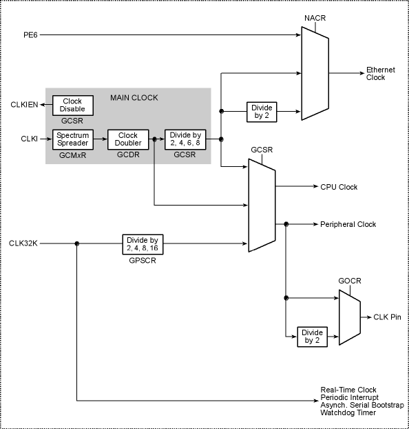
The Rabbit 4000 supports up to three separate clocks—the main clock, the 32 kHz clock, and the 20 MHz Ethernet clock. The main clock is used to derive the processor clock and the peripheral clock inside the processor. The 32 kHz clock is used to drive the asynchronous serial bootstrap, the real-time clock, the periodic interrupt, and the watchdog timers.
The Rabbit 4000 has a spectrum spreader on the main clock that shortens and lengthens clock cycles. This has the net effect of reducing the peak energy of clock harmonics by spreading the spectral energy into nearby frequencies, which reduces EMI and facilitates government-mandated EMI testing. Gated clocks are used whenever possible to avoid clocking unused portions of the processor, and separate power-supply pins for the core and I/O ring further reduce EMI from the Rabbit 4000.
The main clock can be doubled or divided by 2, 4, 6, or 8 to reduce EMI and power consumption. The 32 kHz clock (which can be divided by 2, 4, 8, or 16) can be used instead of the main clock to generate processor and peripheral clocks as low as 2 kHz for significant power savings. Note that dividing the 32 kHz clock only affects the processor and peripheral clocks; the full 32 kHz signal is still provided to the peripherals (RTC and watchdog timers) that use it directly. The periodic interrupt is automatically disabled since there is not enough time to process it when running off the 32 kHz clock.
The Ethernet clock can be driven by the processor clock, the processor clock divided by 2, or by the input on PE6. The Ethernet clock needs to be 20 MHz to conform to the 10Base-T specification. See Chapter 20 for more details on the Ethernet clock.
2.1.1 Block Diagram
2.1.2 Registers
Global Control/Status Register
Global Clock Modulator 0 Register
Global Clock Modulation 1 Register
Global Clock Double Register
2.2 Dependencies
2.2.1 I/O Pins
The main clock input is on the CLKI pin. There is an internal Schmitt trigger on this pin to remove problems with noise on slowly-transitioning signals.
The main clock disable output is on the CLKIEN pin. Its state is changed by one of the bit combinations of bits 4:2 in GCSR.
The 32 kHz clock input is on the CLK32K pin. There is an internal Schmitt trigger on this pin as well.
The peripheral clock or peripheral clock divided by 2 may be optionally output on the CLK pin by enabling it via bits 7:6 in GOCR.
The Ethernet clock may be input on pin PE6 by enabling it via bits 7:6 in NACR. It may be set to use the processor clock or processor clock divided by 2 in that register as well. Note that there is not an internal Schmitt trigger on PE6; it is highly recommended that an external Schmitt trigger be placed on this pin if it is to be used as the Ethernet clock.
2.2.2 Other Registers
GOCR
Used to set up the CLK output pin.
NACR
Used to set up the Ethernet clock.
2.3 Operation
2.3.1 Main Clock
The main clock is input on the CLKI pin, and is optionally sent through the spectrum spreader and then the clock doubler. Both of these are described in greater detail below.
Different main clock modes may be selected via the GCSR, as shown in Table 2-1. Note that one GCSR setting slows the processor clock while the peripheral clock operates at full speed; this allows some power reduction while keeping settings like serial baud rates and the PWM at their desired values.
When the 32 kHz clock is enabled in GCSR, it can be further divided by 2, 4, 6, or 8 to generate even lower frequencies by enabling those modes in bits 0–2 of GPSCR. See Table 2-4 for more details.
2.3.2 Spectrum Spreader
When enabled, the spectrum spreader stretches and compresses the main clock in a complex pattern that spreads the energy of the clock harmonics over a wider range of frequencies.
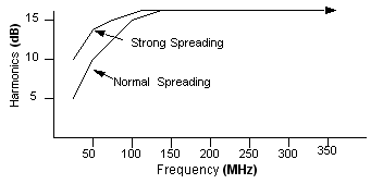
There are three settings that correspond to normal and strong spreading in the 0–50 MHz and >50 MHz main clock range. Each setting will affect the clock cycle differently; the maximum cycle shortening (at 1.8 V and 25°C) is shown in Table 2-2 below.
The spectrum spreader either stretches or shrinks the low plateau of the clock by a maximum of 3 ns for the normal spreading and up to 5 ns for the strong spreading. If the clock doubler is used, this will cause an additional asymmetry between alternate clock cycles.
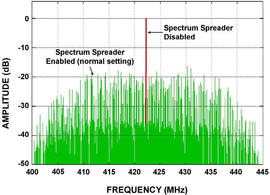
Both normal and strong modes reduce clock harmonics by approximately 15 dB for frequencies above 100 MHz; for lower frequencies the strong setting has a greater effect in reducing the peak spectral strength as shown in Figure 2-2.
Two registers control the clock spectrum spreader. These registers must be loaded in a specific manner with proper time delays. GCM0R is only read by the spectrum spreader at the moment when the spectrum spreader is enabled by storing 0x080 in GCM1R. If GCM1R is cleared (when disabling the spectrum spreader), there is up to a 500-clock delay before the spectrum spreader is actually disabled. The proper procedure is to clear GCM1R, wait for 500 clocks, set GCM0R, and then enable the spreader by storing 0x080 in GCM1R.
The spectrum spreader is applied to the main clock before the clock doubler, so if both are enabled there will be additional asymmetry between alternate clock cycles.If the clock doubler is used, the spectrum spreader affects every other cycle and reduces the clock high time. If the doubler is not used, then the spreader affects every clock cycle, and the clock low time is reduced.
2.3.3 Clock Doubler
The clock doubler allows a lower frequency crystal to be used for the main oscillator and to provide an added range over which the clock frequency can be adjusted. The clock doubler is controlled via the Global Clock Double Register (GCDR).
The clock doubler uses an on-chip delay circuit that must be programmed by the user at startup if there is a need to double the clock. Table 2-3 lists the recommended delays for the GCDR for various oscillator frequencies.
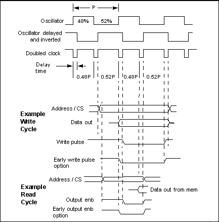
Table 2-3. Recommended Delays Set In GCDR for Clock Doubler When the clock doubler is used and there is no subsequent division of the clock, the output clock will be asymmetric, as shown in Figure 2-3.
The doubled-clock low time is subject to wide (50%) variation since it depends on process parameters, temperature, and voltage. The times given above are for a core supply voltage of 1.8 V and a temperature of 25°C. The values increase or decrease by 1% for each 5°C increase or decrease in temperature. The doubled clock is created by xor'ing the delayed and inverted clock with itself. If the original clock does not have a 50-50 duty cycle, then alternate clocks will have a slightly different length. Since the duty cycle of the built-in oscillator can be as asymmetric as 52% / 48%, the clock generated by the clock doubler will exhibit up to a 4% variation in period on alternate clocks. Memory access time is not affected because memory bus cycle is 2 clocks long and includes both a long and a short clock, resulting in no net change due to asymmetry. However, if an odd number of wait states is used, then the memory access time will be affected slightly
The maximum allowed clock speed must be slightly reduced if the clock is supplied via the clock doubler. The only signals clocked on the falling edge of the clock are the memory and I/O write pulses and the early option memory output enable. See Chapter 5 for more information on the early output enable and write enable options.
The power consumption is proportional to the clock frequency, and for this reason power can be reduced by slowing the clock when less computing activity is taking place. The clock doubler provides a convenient method of temporarily speeding up or slowing down the clock as part of a power management scheme.
2.3.4 32 kHz Clock
The 32.768 kHz clock is used to drive the asynchronous serial bootstrap, the real-time clock, the periodic interrupt, and the watchdog timers. If these features are not used in a design, the use of the 32 kHz clock is optional.
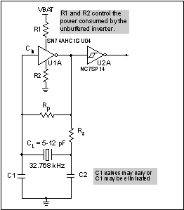
A simplified version of the recommended oscillator circuit for the Rabbit 4000 is shown below. The values of resistors and capacitors may need to be adjusted for various frequencies and crystal load capacitances. Technical Note TN235, "External 32.768 kHz Oscillator Circuits", is available on the Rabbit Semiconductor web site and goes into this circuit in detail.
The 32.768 kHz circuit consumes microampere level currents and has a very high impedance, making it susceptible to noise, moisture, and environmental contaminants. It is strongly recommended to conformally coat this circuit to limit effects of temperature and humidity on the oscillation frequency. Details about this requirement are available in Technical Note TN303, "Conformal Coating", from the Rabbit Semiconductor Web site.
The 32.768 kHz oscillator is slow to start oscillating after power-on. For this reason, a wait loop in the BIOS waits until this oscillator is oscillating regularly before continuing the startup procedure. If the clock is battery-backed, there will be no startup delay since the oscillator is already oscillating. The startup delay may be as much as 5 seconds. Crystals with low series resistance (R < 35 kohms) will start faster.
The 32 kHz oscillator can be used to drive as the processor and peripheral clock to provide significant power savings in "ultra-sleepy" modes. The 32 kHz oscillator can be divided by 2, 4, 8, or 16 to provide clock speeds as low as 2.048 kHz. Special self-timed chip selects are available to keep the memory devices enabled for as short a time as possible when an ultra-sleepy mode is enabled; see Chapter 26 for more details on reducing power consumption.
Table 2-4. Ultra-Sleepy Clock Modes
When the 32 kHz clock is enabled, the periodic interrupt is disabled automatically. The real-time clock and watchdog timers keep running, and use the full 32 kHz clock even when the processor and peripheral clocks use a divider on the 32 kHz clock.
2.4 Register Descriptions
| Rabbit Semiconductor www.rabbit.com |