User's Manual
|
|
| Rabbit 4000 Microprocessor User's Manual |
|
3. Reset and Bootstrap
3.1 Overview
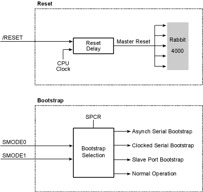
The Rabbit 4000's /RESET pin initializes everything in the processor except for the real-time clock registers and the contents of the battery-backed onchip-encryption RAM. If a write cycle is in progress, it waits until the write cycle is completed to avoid potential memory corruption.
After reset, the Rabbit 4000 checks the state of the SMODE pins. Depending on their state, it either begins normal operation by fetching instruction bytes from /CS0 and /OE0, or it enters a special bootstrap mode where it fetches bytes from either Serial Port A or the slave port. In this mode, bytes can be written to internal registers to set up the Rabbit 4000 for a particular configuration, or to memory to load a program. The processor can begin normal operation once the bootstrap operation is completed.
3.1.1 Block Diagram
3.1.2 Registers
Slave Port Control Register
3.2 Dependencies
3.2.1 I/O Pins
SMODE0, SMODE1 — When the Rabbit 4000 is first powered up or when it is reset, the state of the SMODE0 and SMODE1 pins controls its operation.
/RESET — Pulling the /RESET pin low will initialize everything in the Rabbit 4000 except for the real-time clock registers and the onchip-encryption RAM.
/CS1 — During reset the impedance of the /CS1 pin is high, and all other memory and I/O control signals are held high. The special behavior of /CS1 allows an external RAM to be powered by the same source as the VBATIO pin (which powers /CS1). In this case, a pullup resistor is required on /CS1 to keep the RAM deselected during powerdown.
RESOUT — The RESOUT pin is high during reset and powerdown, but low at all other times, and can be used to control an external power switch to disconnect VDDIO from VBATIO when the main power source is removed.
3.2.2 Clocks
The processor requires a 32 kHz clock input to generate the 2400 bps internal clock required for asynchronous serial bootstrap. No 32 kHz clock is required for either clocked serial or slave port bootstrap.
When the processor comes out of reset, the CPU clock and peripheral clocks are both in divide-by-8 mode.
3.2.3 Other Registers
SPCR
Enable/disable processor monitoring of SMODE pins; read current state of SMODE pins.
3.2.4 Interrupts
There are no interrupts associated with reset or bootstrap.
3.3 Operation
Pulling the /RESET pin low will initialize everything in the Rabbit 4000 except for the real-time clock registers and the onchip-encryption RAM. The reset of the Rabbit 4000 is delayed until the completion of any write cycles in progress; reset takes effect immediately when no write cycles are occurring. The reset sequence requires a minimum of 128 cycles of the main clock to complete in either case.
During reset, the impedance of the /CS1 pin is high and all other memory and I/O control signals are held high. The special behavior of /CS1 allows an external RAM to be powered by the same source as the VBATIO pin (which powers /CS1). In this case, a pullup resistor is required on /CS1 to keep the RAM deselected during powerdown. The RESOUT pin is high during reset and powerdown, but low at all other times, and can be used to control an external power switch to disconnect VDDIO from VBATIO when the main power source is removed.
Table 3-1 lists the condition of the processor after reset takes place. The state of all registers after reset is provided in the chapter describing the specific peripheral.
Table 3-1. Rabbit 4000 Condition After Reset
The processor checks the SMODE pins after the /RESET signal is inactive. Table 3-2 summarizes what happens:
- If both SMODE pins are zero, the Rabbit 4000 begins fetching instructions from the memory device on /CS0 and /OE0. If a 16-bit memory is used on /CS0, the first section of code must immediately select the 16-bit bus mode. Chapter 5 provides a short program to do this.
- If either of the SMODE pins is high, the processor will enter the bootstrap mode and accept triplets from either Serial Port A or the slave port. It is good practice to place pulldown resistors on the SMODE pins to ensure proper operation of your design.
In bootstrap mode, the processor inhibits the normal memory fetch from /CS0 and instead fetches instructions from a small internal boot ROM. This program reads triplets of three bytes from the selected peripheral. The first byte is the most-significant byte of a 16-bit address, the second byte is the least-significant byte of the address, and the third byte is the data to be written. If the uppermost bit of the address is 1, then the address is assumed to be an internal register address instead of a memory address, and the data are written to the appropriate register instead.
The boot ROM program waits for data to be available; each byte received automatically resets the watchdog timer with a 2-second timeout. Bytes must be received quickly enough to prevent timeout (or the watchdog must be disabled).
The device checks the state of the SMODE pins each time it jumps back to the start of the ROM program and responds according to the current state. In addition, by writing to bit 7 of the Slave Port Control Register (SPCR) the processor can be told to ignore the state of the SMODE pins and continue normal operation.
Note that the processor can be told to reenter bootstrap mode at any time by setting bit 7 of SPCR low; once this occurs and the least-significant four bits of the current PC address are zero, the processor will sample the state of the SMODE pins and respond accordingly. This feature allows in-line downloading from the selected bootstrap port; once the download is complete, bit 7 of SPCR can be set high and the processor will continue operating from where it left off.
As a security feature, any attempt to enter bootstrap mode from either the SMODE pins or by writing to bit 7 of SPCR will erase the data stored in the onchip-encryption RAM. This prevents loading a small program in memory to read out the data.
3.4 Register Descriptions
| Rabbit Semiconductor www.rabbit.com |