24. External I/O Control
24.1 Overview
The Rabbit 4000's external I/O space consists of 64KB that is accessed by prefixing a read or write instruction with the IOE instruction. These accesses can go onto the memory bus or onto the external I/O bus (described below). There are three dedicated signal pins (/IORD, /IOWR, /BUFEN) that toggle for all external I/O accesses, and eight I/O strobes that can be associated with this external I/O space and directed out of Parallel Ports C, D, or E.
In addition, a handshaking signal input can be enabled on a Parallel Port E pin, and used to pause an external I/O transaction until the external device is ready to complete the transaction. A timeout period can be defined to ensure that the processor is not held indefinitely by a misbehaving external device.
24.1.1 Auxiliary I/O Bus
The Rabbit 4000 can enable a separate auxiliary I/O bus for external devices to keep bus loading on the memory bus at an acceptable level. This bus consists of eight data lines on Parallel Port A and up to eight address lines on Parallel Port B. This functionality is mutually exclusive with the slave port and regular parallel I/O on Parallel Ports A and B.
When enabled, the address lines of the auxiliary I/O bus hold their value until a new value is written to them. The data lines return to a tristate mode after each transaction.
See Section 24.1.2 for memory timing for external I/O accesses.
24.1.2 I/O Strobes
There are eight I/O strobes available in the Rabbit 4000. Each has a separate 8KB address range that can be enabled as a chip select, read strobe, write strobe, or a read/write strobe. The number of wait states can be set to 1, 3, 7, or 15, and the signal can be active high or low.
Table 24-1. External I/O Strobes
|
|
External I/O Address Range
|
|
|
|
|
|
|
|
|
|
|
|
|
|
|
|
|
|
|
|
|
|
|
|
|
The I/O strobes can be used for devices on the memory bus or the auxiliary I/O bus, and can be enabled to go out on the memory bus alone or both buses. It is also possible to shorten the read strobe by one clock cycle and the write strobe by one-half a clock cycle by pulling in the trailing edge, which guarantees one clock cycle of hold time for transactions.
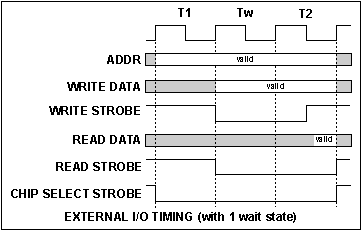
Figure 24-1. Auxiliary I/O Bus Cycles
The strobes can be enabled to come out on Parallel Ports C, D, or E.
By default the I/O strobes are configured as read-only chip selects with 15 wait states and normal timing. These settings will affect the /IORD, /IOWR, and /BUFEN signals for external I/O writes even if no other strobe outputs are enabled in the parallel port registers.
24.1.3 I/O Handshake
An external I/O handshake input can be enabled on one of the Parallel Port E pins for any combination of the I/O banks. The external device holds this signal (active high or low) when it is busy and cannot accept a transaction. The Rabbit 4000 will then hold midway through the transaction until either the handshake signal goes inactive or a timeout occurs. The timeout can be defined anywhere from 32 to 2048 clocks. When the timeout occurs, the transaction ends and a status bit is set. This bit must be checked by the program attempting the write; no interrupt is generated.
The I/O handshake signal is sampled at the end of the first wait state (Tw). When the handshake signal is disabled, the transition will start at the beginning of the Tw phase and continue to completion.
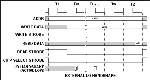
Figure 24-2. External I/O Handshake Timing Diagram
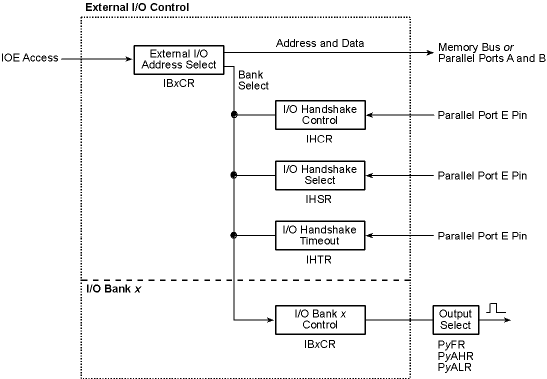
24.1.4 Block Diagram
24.1.5 Registers
|
I/O Handshake Control Register
|
|
|
|
|
I/O Handshake Select Register
|
|
|
|
|
I/O Handshake Timeout Register
|
|
|
|
|
I/O Bank 0 Control Register
|
|
|
|
|
I/O Bank 1 Control Register
|
|
|
|
|
I/O Bank 2 Control Register
|
|
|
|
|
I/O Bank 3 Control Register
|
|
|
|
|
I/O Bank 4 Control Register
|
|
|
|
|
I/O Bank 5 Control Register
|
|
|
|
|
I/O Bank 6 Control Register
|
|
|
|
|
I/O Bank 7 Control Register
|
|
|
|
|
24.2 Dependencies
24.2.1 I/O Pins
The auxiliary I/O bus uses PA0–PA7 for data, and either PB2–PB7 or PB0–PB7 for address lines, depending on the setting in SPCR. Address bits 6 and 7 can also be enabled on pins PD1, PD3, PD5, or PD7, which allows PB0 and PB1 to be used as clocked serial I/O instead of as external I/O..
The /IOWR, /IORD, and /BUFEN pins are dedicated strobes for external I/O accesses.
The I/O strobes can be directed out to pins on Parallel Ports C, D, or E; each bank can be directed to the appropriate pin (bank zero on PC0, PD0, or PE0; bank one on PC1, PD1, or PE1; etc.). The strobes will affect outputs on /IOWR, /IORD, and /BUFEN at all times.
The I/O handshake can be input on any one of the Parallel Port E pins (PE0–PE7).
24.2.2 Clocks
All external I/O accesses, strobes, and handshake timeouts are based on the processor clock.
24.2.3 Other Registers
|
SPCR
|
Enable the auxiliary I/O bus.
|
PCFR, PCALR, PCAHR
PDFR, PDALR, PDAHR,
PEFR, PEALR, PEAHR
|
Select Parallel Port C, D, or E pins as I/O strobe outputs.
Select PD1, PD3, PD5, or PD7 as address bits 6-7.
|
24.2.4 Interrupts
There are no interrupts associated with external I/O.
24.3 Operation
24.3.1 Auxiliary I/O Bus
The following steps must be taken before using auxiliary I/O bus:
- Enable the auxiliary I/O bus by writing to SPCR. Select whether 6 or 8 address bits are desired.
- If PB0 and PB1 are needed for clocked serial use and eight address bits are required, enable the alternate outputs of address bits 6 and 7 on Parallel Port D by writing to PDALR, PDAHR, and PDFR.
- Set the I/O timing for a particular device by writing to the appropriate IBxCR register for the I/O bank desired.
- If a strobe other than /IORD, /IOWR, or /BUFEN is required, enable the output of the IBxCR register by writing to the appropriate PxALR, PxAHR, and PxFR registers.
Once the auxiliary I/O bus is enabled, all memory read/write instructions prefixed with an IOE will go to either the memory bus or auxiliary I/O bus, depending on the setup in that bank's IBxCR register.
24.3.2 I/O Strobes
The following steps must be taken before using an I/O strobe:
- Set the strobe type and timing for a particular device by writing to the appropriate IBxCR register for the I/O bank desired.
- If signals other than /IORD, /IOWR, and /BUFEN are required, enable the output of the IBxCR register by writing to the appropriate PxALR, PxAHR, and PxFR registers.
On startup, the I/O strobes are set as chip selects with 15 wait states, read-only, active-low signaling, and will use the auxiliary I/O bus. These settings will be used for the dedicated I/O strobe pins /IORD, /IOWR, and /BUFEN whenever an external I/O write occurs even if not I/O strobe signals are being output on parallel port pins.
24.3.3 I/O Handshake
The following steps must be taken before using the I/O handshake:
- Select the active level and desired port E bit to use as input by writing to IHCR.
- Select which I/O banks the handshake is active for by writing to IHSR.
- Select the handshake timeout value by writing to IHTR.
Once enabled, the handshake will be checked for every external I/O transaction in a bank that was enabled in IHSR. After these transactions, the program should check for a timeout by reading IHTR.
24.4 Register Descriptions
|
I/O Handshake Control Register (IHCR) (Address = 0x0028)
|
|
|
|
|
|
|
|
These bits are reserved and should be written with zeros.
|
|
|
|
I/O handshake is active low (I/O transaction held until signal goes high).
|
|
|
|
I/O handshake is active high (I/O transaction held until signal goes low).
|
|
|
|
This bit is reserved and should be written with zero.
|
|
|
|
Use Parallel Port E bit 0 for I/O handshake.
|
|
|
|
Use Parallel Port E bit 1 for I/O handshake.
|
|
|
|
Use Parallel Port E bit 2 for I/O handshake.
|
|
|
|
Use Parallel Port E bit 3 for I/O handshake.
|
|
|
|
Use Parallel Port E bit 4 for I/O handshake.
|
|
|
|
Use Parallel Port E bit 5 for I/O handshake.
|
|
|
|
Use Parallel Port E bit 6 for I/O handshake.
|
|
|
|
Use Parallel Port E bit 7 for I/O handshake.
|
|
I/O Handshake Select Register (IHSR) (Address = 0x0029)
|
|
|
|
|
|
|
|
Disable I/O handshake for I/O Bank 7.
|
|
|
|
Enable I/O handshake for I/O Bank 7.
|
|
|
|
Disable I/O handshake for I/O Bank 6.
|
|
|
|
Enable I/O handshake for I/O Bank 6.
|
|
|
|
Disable I/O handshake for I/O Bank 5.
|
|
|
|
Enable I/O handshake for I/O Bank 5.
|
|
|
|
Disable I/O handshake for I/O Bank 4.
|
|
|
|
Enable I/O handshake for I/O Bank 4.
|
|
|
|
Disable I/O handshake for I/O Bank 3.
|
|
|
|
Enable I/O handshake for I/O Bank 3.
|
|
|
|
Disable I/O handshake for I/O Bank 2.
|
|
|
|
Enable I/O handshake for I/O Bank 2.
|
|
|
|
Disable I/O handshake for I/O Bank 1.
|
|
|
|
Enable I/O handshake for I/O Bank 1.
|
|
|
|
Disable I/O handshake for I/O Bank 0.
|
|
|
|
Enable I/O handshake for I/O Bank 0.
|
|
I/O Handshake Timeout Register (IHTR) (Address = 0x002A)
|
|
|
|
|
|
|
|
No I/O handshake timeout has occurred since the last read of this register.
|
|
|
|
An I/O handshake timeout has occured since the last read of this register. This bit is cleared by a read of this register.
|
|
|
|
This bit is reserved and should be written with zero.
|
|
|
|
Time constant for the I/O handshake timeout counter. This time constant (times 32) selects the number of clocks that the I/O handshake input may delay completion of an I/O transaction before the I/O transaction will complete automatically.
|
|
I/O Bank x Control Register (IB0CR) (Address = 0x0080)
(IB1CR) (Address = 0x0081)
(IB2CR) (Address = 0x0082)
(IB3CR) (Address = 0x0083)
(IB4CR) (Address = 0x0084)
(IB5CR) (Address = 0x0085)
(IB6CR) (Address = 0x0086)
(IB7CR) (Address = 0x0087)
|
|
|
|
|
|
|
|
Fifteen wait states for accesses in this bank.
|
|
|
|
Seven wait states for accesses in this bank.
|
|
|
|
Three wait states for accesses in this bank.
|
|
|
|
One wait state for accesses in this bank.
|
|
|
|
The I signal is an I/O chip select.
|
|
|
|
The I signal is an I/O read strobe.
|
|
|
|
The I signal is an I/O write strobe.
|
|
|
|
The I signal is an I/O data (read or write) strobe.
|
|
|
|
Writes are not allowed to this bank. Transactions are normal in every other way; only the write strobe is inhibited.
|
|
|
|
Writes are allowed to this bank.
|
|
|
|
Active-low I signal.
|
|
|
|
Inverted (active-high) I signal.
|
|
|
|
Normal I/O transaction timing.
|
|
|
|
Shorten read strobe by one clock cycle and write strobe by one-half clock cycle. Transaction length remains the same. This guarantees one clock cycle hold time for both address and data for I/O transactions.
|
|
|
|
Use I/O bus if enabled.
|
|
|
|
Always use memory data bus.
|
|
Slave Port Control Register (SPCR) (Address = 0x0024)
|
|
|
|
|
|
|
|
Program fetch as a function of the SMODE pins.
|
|
|
|
Ignore the SMODE pins program fetch function.
|
|
|
|
These bits report the state of the SMODE pins.
|
|
|
|
These bits are ignored and should be written with zero.
|
|
|
|
Disable the slave port. Parallel Port A is a byte-wide input port.
|
|
|
|
Disable the slave port. Parallel Port A is a byte-wide output port.
|
|
|
|
Enable the slave port, with /SCS from Parallel Port E bit 7.
|
|
|
|
Enable the auxiliary I/O bus. Parallel Port A is used for the data bus and Parallel Port B[7:2] is used for the address bus.
|
|
|
|
This bit combination is reserved and should not be used.
|
|
|
|
This bit combination is reserved and should not be used.
|
|
|
|
Enable the slave port, with /SCS from Parallel Port B bit 6.
|
|
|
|
Enable the auxiliary I/O bus. Parallel Port A is used for the data bus and Parallel Port B[7:0] is used for the address bus.
|
|
|
|
Slave port interrupts are disabled.
|
|
|
|
Slave port interrupts use Interrupt Priority 1.
|
|
|
|
Slave port interrupts use Interrupt Priority 2.
|
|
|
|
Slave port interrupts use Interrupt Priority 3.
|
|
Parallel Port C Alternate Low Register (PCALR) (Address = 0x0052)
|
|
|
|
|
|
|
|
Parallel Port C bit 3 alternate output 0 (TXC).
|
|
|
|
Parallel Port C bit 3 alternate output 1 (I3).
|
|
|
|
Parallel Port C bit 3 alternate output 2 (TIMER C3).
|
|
|
|
Parallel Port C bit 3 alternate output 3 (SCLKD).
|
|
|
|
Parallel Port C bit 2 alternate output 0 (TXC).
|
|
|
|
Parallel Port C bit 2 alternate output 1 (I2).
|
|
|
|
Parallel Port C bit 2 alternate output 2 (TIMER C2).
|
|
|
|
Parallel Port C bit 2 alternate output 3 (TXF).
|
|
|
|
Parallel Port C bit 1 alternate output 0 (TXD).
|
|
|
|
Parallel Port C bit 1 alternate output 1 (I1).
|
|
|
|
Parallel Port C bit 1 alternate output 2 (TIMER C1).
|
|
|
|
Parallel Port C bit 1 alternate output 3 (RCLKF).
|
|
|
|
Parallel Port C bit 0 alternate output 0 (TXD).
|
|
|
|
Parallel Port C bit 0 alternate output 1 (I0).
|
|
|
|
Parallel Port C bit 0 alternate output 2 (TIMER C0).
|
|
|
|
Parallel Port C bit 0 alternate output 3 (TCLKF).
|
|
Parallel Port C Alternate High Register (PCAHR) (Address = 0x0053)
|
|
|
|
|
|
|
|
Parallel Port C bit 7 alternate output 0 (TXA).
|
|
|
|
Parallel Port C bit 7 alternate output 1 (I7).
|
|
|
|
Parallel Port C bit 7 alternate output 2 (PWM3).
|
|
|
|
Parallel Port C bit 7 alternate output 3 (SCLKC).
|
|
|
|
Parallel Port C bit 6 alternate output 0 (TXA).
|
|
|
|
Parallel Port C bit 6 alternate output 1 (I6).
|
|
|
|
Parallel Port C bit 6 alternate output 2 (PWM2).
|
|
|
|
Parallel Port C bit 6 alternate output 3 (TXE).
|
|
|
|
Parallel Port C bit 5 alternate output 0 (TXB).
|
|
|
|
Parallel Port C bit 5 alternate output 1 (I5).
|
|
|
|
Parallel Port C bit 5 alternate output 2 (PWM1).
|
|
|
|
Parallel Port C bit 5 alternate output 3 (RCLKE).
|
|
|
|
Parallel Port C bit 4 alternate output 0 (TXB).
|
|
|
|
Parallel Port C bit 4 alternate output 1 (I4).
|
|
|
|
Parallel Port C bit 4 alternate output 2 (PWM0).
|
|
|
|
Parallel Port C bit 4 alternate output 3 (TCLKE).
|
|
Parallel Port C Function Register (PCFR) (Address = 0x0055)
|
|
|
|
|
|
|
|
The corresponding port bit functions normally.
|
|
|
|
The corresponding port bit carries its alternate signal as an output. See Table 10-1.
|
|
Parallel Port D Alternate Low Register (PDALR) (Address = 0x0062)
|
|
|
|
|
|
|
|
Parallel Port D bit 3 alternate output 0 (IA7).
|
|
|
|
Parallel Port D bit 3 alternate output 1 (I3).
|
|
|
|
Parallel Port D bit 3 alternate output 2 (TIMER C3).
|
|
|
|
Parallel Port D bit 3 alternate output 3 (SCLKD).
|
|
|
|
Parallel Port D bit 2 alternate output 0 (SCLKC).
|
|
|
|
Parallel Port D bit 2 alternate output 1 (I2).
|
|
|
|
Parallel Port D bit 2 alternate output 2 (TIMER C2).
|
|
|
|
Parallel Port D bit 2 alternate output 3 (TXF).
|
|
|
|
Parallel Port D bit 1 alternate output 0 (IA6).
|
|
|
|
Parallel Port D bit 1 alternate output 1 (I1).
|
|
|
|
Parallel Port D bit 1 alternate output 2 (TIMER C1).
|
|
|
|
Parallel Port D bit 1 alternate output 3 (RCLKF).
|
|
|
|
Parallel Port D bit 0 alternate output 0 (SCLKD).
|
|
|
|
Parallel Port D bit 0 alternate output 1 (I0).
|
|
|
|
Parallel Port D bit 0 alternate output 2 (TIMER C0).
|
|
|
|
Parallel Port D bit 0 alternate output 3 (TCLKF).
|
|
Parallel Port D Alternate High Register (PDAHR) (Address = 0x0063)
|
|
|
|
|
|
|
|
Parallel Port D bit 7 alternate output 0 (IA7).
|
|
|
|
Parallel Port D bit 7 alternate output 1 (I7).
|
|
|
|
Parallel Port D bit 7 alternate output 2 (PWM3).
|
|
|
|
Parallel Port D bit 7 alternate output 3 (SCLKC).
|
|
|
|
Parallel Port D bit 6 alternate output 0 (TXA).
|
|
|
|
Parallel Port D bit 6 alternate output 1 (I6).
|
|
|
|
Parallel Port D bit 6 alternate output 2 (PWM2).
|
|
|
|
Parallel Port D bit 6 alternate output 3 (TXE).
|
|
|
|
Parallel Port D bit 5 alternate output 0 (IA6).
|
|
|
|
Parallel Port D bit 5 alternate output 1 (I5).
|
|
|
|
Parallel Port D bit 5 alternate output 2 (PWM1).
|
|
|
|
Parallel Port D bit 5 alternate output 3 (RCLKE).
|
|
|
|
Parallel Port D bit 4 alternate output 0 (TXB).
|
|
|
|
Parallel Port D bit 4 alternate output 1 (I4).
|
|
|
|
Parallel Port D bit 4 alternate output 2 (PWM0).
|
|
|
|
Parallel Port D bit 4 alternate output 3 (TCLKE).
|
|
Parallel Port D Function Register (PDFR) (Address = 0x0065)
|
|
|
|
|
|
|
|
The corresponding port bit functions normally.
|
|
|
|
The corresponding port bit carries its alternate signal as an output. See Table 11-1.
|
|
Parallel Port E Alternate Low Register (PEALR) (Address = 0x0072)
|
|
|
|
|
|
|
|
Parallel Port E bit 3 alternate output 0 (I3).
|
|
|
|
Parallel Port E bit 3 alternate output 1 (A23).
|
|
|
|
Parallel Port E bit 3 alternate output 2 (TIMER C3).
|
|
|
|
Parallel Port E bit 3 alternate output 3 (SCLKD).
|
|
|
|
Parallel Port E bit 2 alternate output 0 (I2).
|
|
|
|
Parallel Port E bit 2 alternate output 1 (A22).
|
|
|
|
Parallel Port E bit 2 alternate output 2 (TIMER C2).
|
|
|
|
Parallel Port E bit 2 alternate output 3 (TXF).
|
|
|
|
Parallel Port E bit 1 alternate output 0 (I1).
|
|
|
|
Parallel Port E bit 1 alternate output 1 (A21).
|
|
|
|
Parallel Port E bit 1 alternate output 2 (TIMER C1).
|
|
|
|
Parallel Port E bit 1 alternate output 3 (RCLKF).
|
|
|
|
Parallel Port E bit 0 alternate output 0 (I0).
|
|
|
|
Parallel Port E bit 0 alternate output 1 (A20).
|
|
|
|
Parallel Port E bit 0 alternate output 2 (TIMER C0).
|
|
|
|
Parallel Port E bit 0 alternate output 3 (TCLKF).
|
|
Parallel Port E Alternate High Register (PEAHR) (Address = 0x0073)
|
|
|
|
|
|
|
|
Parallel Port E bit 7 alternate output 0 (I7).
|
|
|
|
Parallel Port E bit 7 alternate output 1 (/ACT).
|
|
|
|
Parallel Port E bit 7 alternate output 2 (PWM3).
|
|
|
|
Parallel Port E bit 7 alternate output 3 (SCLKC).
|
|
|
|
Parallel Port E bit 6 alternate output 0 (I6).
|
|
|
|
Parallel Port E bit 6 alternate output 1 (—).
|
|
|
|
Parallel Port E bit 6 alternate output 2 (PWM2).
|
|
|
|
Parallel Port E bit 6 alternate output 3 (TXE).
|
|
|
|
Parallel Port E bit 5 alternate output 0 (I5).
|
|
|
|
Parallel Port E bit 5 alternate output 1 (/LINK).
|
|
|
|
Parallel Port E bit 5 alternate output 2 (PWM1).
|
|
|
|
Parallel Port E bit 5 alternate output 3 RCLKE).
|
|
|
|
Parallel Port E bit 4 alternate output 0 (I4).
|
|
|
|
Parallel Port E bit 4 alternate output 1 (/A0).
|
|
|
|
Parallel Port E bit 4 alternate output 2 (PWM0).
|
|
|
|
Parallel Port E bit 4 alternate output 3 (TCLKE).
|
|
Parallel Port E Function Register (PEFR) (Address = 0x0075)
|
|
|
|
|
|
|
|
The corresponding port bit functions normally.
|
|
|
|
The corresponding port bit carries its alternate signal as an output. See Table 12-1.
|
