User's Manual
|
|
| Rabbit 4000 Microprocessor User's Manual |
|
23. Pulse Width Modulator
23.1 Overview
The Pulse Width Modulator (PWM) consists of a 10-bit free running counter and four width registers. A PWM output consists of a train of periodic pulses within a 1024-count frame with a duty cycle that varies from 1/1024 to 1024/1024. Each PWM output is high for n + 1 counts out of the 1024-clock count cycle, where n is the value held in the width register. The PWM is clocked by the output of Timer A9 which is used to set the period.
Each PWM output high time can optionally be spread throughout the cycle to reduce ripple on the externally filtered PWM output. The PWM outputs can be passed through a filter and used as a 10-bit D/A converter. The outputs can also be used to directly drive devices such as motors or solenoids that have intrinsic filtering.
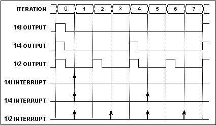
The PWM outputs can trigger a PWM interrupt on every PWM cycle, every other cycle, every fourth cycle, or every eighth cycle. In addition, the PWM output can be suppressed every other cycle, three out of every four cycles, or seven out of every eight cycles. These options provide support for driving servos and to generate audio signals. The setup for this interrupt is done in the PWL0R and PWL1R registers. The timing is shown below.
The spreading function is implemented by dividing each 1024-clock cycle into four quadrants of 256 clocks each. Within each quadrant, the Pulse-Width Modulator uses the eight MSBs of each pulse-width register to select the base width in each of the quadrants. This is the equivalent to dividing the contents of the pulse-width register by four and using this value in each quadrant. To get the exact high time, the Pulse-Width Modulator uses the two LSBs of the pulse-width register to modify the high time in each quadrant according to the table below. The "n/4" term is the base count, formed from the eight MSBs of the pulse-width register.
n/4 + 1
n/4
n/4
n/4
n/4 + 1
n/4
n/4 + 1
n/4
n/4 + 1
n/4 + 1
n/4 + 1
n/4
n/4 + 1
n/4 + 1
n/4 + 1
n/4 + 1
The diagram below shows a PWM output for several different width values, for both modes of operation. Operation in the spread mode reduces the filtering requirements on the PWM output in most cases.
The DMA channels on the Rabbit 4000 are designed to work with fixed I/O addresses. To allow DMA control of the PWM, a separate PWM Block Access Register (PWBAR) and PWM Block Pointer Register (PWBPR) are available. The pointer register contains the address of the PWM register to be accessed via the access register. Each read or write of the access register automatically increments the pointer register through the sequence shown below. Note that only the lower three bits of the pointer register actually change. This allows the DMA to write to a fixed internal I/O location but still program all of the PWM registers. The pointer register can be written and read if necessary. Normally the pointer register is initialized to 0x88 (the first PWM register) and the DMA then transfers blocks of eight bytes to completely reprogram the PWM.
0x88 -> 0x89 -> 0x8A -> 0x8B -> 0x8C -> 0x8D -> 0x8E -> 0x8F ->When the DMA destination address is the PWBAR, the DMA request from the PWM is automatically connected to the DMA.
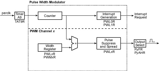
23.1.1 Block Diagram
23.1.2 Registers
23.2 Dependencies
23.2.1 I/O Pins
Each PWM channel can be output on up one of three pins, which can be selected via the parallel port alternate output registers.
Channel 0
Channel 1
Channel 2
Channel 3
23.2.2 Clocks
The PWM counter is clocked from the output of Timer A9, and can run at rates from perclk/2 down to perclk/512 by writing the appropriate value to TAT9R.
23.2.3 Other Registers
TAT9R
Time constant for PWM clock
PCFR, PCAHR
PDFR, PDAHR
PEFR, PEAHR
Alternate port output selection
23.2.4 Interrupts
The PWM can generate an interrupt for every PWM counter rollover, every second rollover, every fourth rollover, or every eighth rollover. This option is selected in PWL1R. The interrupt request is cleared by a write to any PWM register.
The PWM interrupt vector is in the IIR at offset 0x170. It can be set as Priority 1, 2, or 3 by writing to PWL0R.
23.3 Operation
The following steps explain how to set up a PWM channel.
- Configure Timer A9 via TAT9R to provide the desired PWM clock frequency.
- Configure PWLxR to select whether to spread the PWM output throughout the cycle.
- Configure PWLxR to select whether to suppress the PWM output.
- Configure the duty cycle by writing to PWLxR and PWMxR.
23.3.1 Handling Interrupts
The following steps explain how an interrupt is set up and used.
- Write the vector to the interrupt service routine to the internal interrupt table.
- Configure PWL0R to select the PWM interrupt priority and PWL1R to select PWM interrupt suppression (if an interrupt is desired).
The following actions occur within the interrupt service routine.
- Any PWM values may be updated.
- The interrupt request should be cleared by writing to any PWM register.
23.3.2 Example ISR
A sample interrupt handler is shown below.
pwm_isr::
   push af              ; save used registers
   ld a, 0x55
   ioi ld (PWM0R), a     ; update a PWM value
; note that interrupt request is also cleared by register write above
   pop af               ; restore used registers
   ipres
   ret
23.4 Register Descriptions
Most significant eight bits for the Pulse Width Modulator count. With a count of "n", the PWM output will be High for "n + 1" clocks out of the 1024 clocks of the PWM counter.
Access the PWM register pointed to by the PWBPR. The PWBPR is automatically updated to the next PWM register address in the sequence.
These bits are ignored and should be written with zero.
Three least significant bits of the PWM register address for indirect access.
| Rabbit Semiconductor www.rabbit.com |