Rabbit 4000 Microprocessor
User's Manual
PREV INDEX NEXT


12. Parallel Port E

12.1 Overview

Parallel Port E is a byte-wide port with each bit programmable for data direction and drive level. These are simple inputs and outputs controlled and reported in the Port E Data Register (PEDR).

All of the Parallel Port E pins have alternate output functions, and all of them can be used as inputs to various on-chip peripherals.

When used as outputs, the Parallel Port E bits are buffered, with the data written to PEDR transferred to the output pins on a selected timing edge. Either the peripheral clock or the outputs of Timer A1, Timer B1, or Timer B2 can be used for this function, with each nibble of the port having a separate select field to control this timing. Each bit can either be programmed as open-drain or driven high and low.

Because of the buffered nature of Parallel Port E, using a read-modify-write type of operation can lead to old data being written to PEDR. To alleviate this potential problem, each bit of the port can be written individually using a separate address for each bit.

Bit 7 of Parallel Port E is used as the default chip select input for the slave port when the slave port is enabled, either for parallel bootstrap or under program control.

Table 12-1. Parallel Port E Pin Alternate Output Functions

Pin Name

Alt Out 0

Alt Out 1

Alt Out 2

Alt Out 3

PE7
I7
/ACT
PWM3
SCLKC
PE6
I6

PWM2
TXE
PE5
I5
/LINK
PWM1
RCLKE
PE4
I4
/A0
PWM0
TCLKE
PE3
I3
A23
TIMER C3
SCLKD
PE2
I2
A22
TIMER C2
TXF
PE1
I1
A21
TIMER C1
RCLKF
PE0
I0
A20
TIMER C0
TCLKF


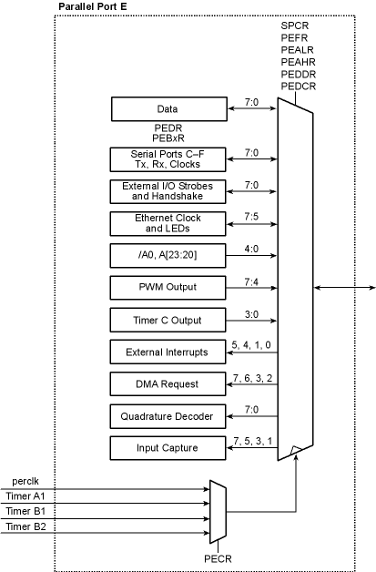
Table 12-2. Parallel Port E Pin Alternate Input Functions

Pin Name

Input Capture

Serial Ports A–D

Serial Ports E–F

DMA

External Interrupts

Quad Decode

Ethernet

PE7
×
RXA
RXE
DREQ1


PE6


DREQ0


ECLK
PE5
×
RXB
RCLKE

INT1


PE4


TCLKE

INT0


PE3
×
RXC
RXF
DREQ1

QRD2A

PE2

SCLKC

DREQ0

QRD2B

PE1
×
RXD
RCLKF

INT1
QRD1A

PE0

SCLKD
TCLKF

INT0
QRD1B

12.1.1 Block Diagram


12.1.2 Registers

Register Name

Mnemonic

I/O Address

R/W

Reset

Port E Data Register
PEDR
0x0070
R/W
xxxxxxxx
Port E Alternate Low Register
PEALR
0x0072
R/W
00000000
Port E Alternate High Register
PEAHR
0x0073
R/W
00000000
Port E Control Register
PECR
0x0074
R/W
xx00xx00
Port E Function Register
PEFR
0x0075
R/W
00000000
Port E Drive Control Register
PEDCR
0x0076
R/W
00000000
Port E Data Direction Register
PEDDR
0x0077
R/W
00000000
Port E Bit 0 Register
PEB0R
0x0078
W
xxxxxxxx
Port E Bit 1 Register
PEB1R
0x0079
W
xxxxxxxx
Port E Bit 2 Register
PEB2R
0x007A
W
xxxxxxxx
Port E Bit 3 Register
PEB3R
0x007B
W
xxxxxxxx
Port E Bit 4 Register
PEB4R
0x007C
W
xxxxxxxx
Port E Bit 5 Register
PEB5R
0x007D
W
xxxxxxxx
Port E Bit 6 Register
PEB6R
0x007E
W
xxxxxxxx
Port E Bit 7 Register
PEB7R
0x007F
W
xxxxxxxx


12.2 Dependencies

12.2.1 I/O Pins

Parallel Port E uses the pins PE0 through PE7. These pins can be used individually as data inputs or outputs; as serial port transmit and receive for Serial Ports E and F; as clocks for Serial Ports C–F; as external I/O strobes; as outputs for the PWM and Timer C peripherals; as the upper address bits A[23:20]; or as the Ethernet clock and status LEDs for the on-chip network peripheral. The input capture peripheral can also watch pins PE7, PE5, PE3, and PE1. There is also an option to provide the slave port chip select on PE7.

All pins are set as inputs on startup.

The individual bits can be set to be open-drain via PEDCR.

See the associated peripheral chapters for details on how they use Parallel Port E.

12.2.2 Clocks

All outputs on Parallel Port E are clocked by the peripheral clock unless changed in PECR, where the option of updating the Parallel Port E pins can be synchronized to the output of Timer A1, Timer B1, or Timer B2.

12.2.3 Other Registers

Register

Function

SACR, SBCR, SCCR, SDCR, SECR, SFCR
Select a Parallel Port E pin as serial data (and optional clock) input.
ICS1R, ICS2R
Select a Parallel Port E pin as a start/stop condition input.
QDCR
Select a Parallel Port E pin as a decoder input.
I0CR, I1CR
Select a Parallel Port E pin as an external interrupt input.
DMR0CR, DMR1CR
Select a Parallel Port E pin as an external DMA request input.
NACR
Select PE6 as the Ethernet clock input.
SPCR
Select slave chip select on PE7.


12.2.4 Interrupts

External interrupts can be accepted from pins PE5, PE4, PE1 or PE0; see Chapter 7 for more details.

12.3 Operation

The following steps must be taken before using Parallel Port E.

  1. Select the desired input/output direction for each pin via PEDDR.

  2. Select high/low or open-drain functionality for outputs via PEDCR.

  3. If an alternative peripheral output function is desired for a pin, select it by via PEALR or PEAHR and then enable it via PEFR. Refer to the appropriate peripheral chapter for further use of that pin.

Once the port is set up, data can be read or written by accessing PEDR. The value of an output pin read in from PEDR will reflect its current output value, but any value written to an input pin will not appear until that pin becomes an output.

12.4 Register Descriptions

Parallel Port E Data Register (PEDR) (Address = 0x0070)

Bit(s)

Value

Description

7:0
Read
The current state of Parallel Port E pins PE7–PE0 is reported.
Write
The Parallel Port E buffer is written with this value for transfer to the Parallel Port E output register on the next rising edge of the peripheral clock.


Parallel Port E Alternate Low Register (PEALR) (Address = 0x0072)

Bit(s)

Value

Description

7:6
00
Parallel Port E bit 3 alternate output 0 (I3).
01
Parallel Port E bit 3 alternate output 1 (A23).
10
Parallel Port E bit 3 alternate output 2 (TIMER C3).
11
Parallel Port E bit 3 alternate output 3 (SCLKD).
5:4
00
Parallel Port E bit 2 alternate output 0 (I2).
01
Parallel Port E bit 2 alternate output 1 (A22).
10
Parallel Port E bit 2 alternate output 2 (TIMER C2).
11
Parallel Port E bit 2 alternate output 3 (TXF).
3:2
00
Parallel Port E bit 1 alternate output 0 (I1).
01
Parallel Port E bit 1 alternate output 1 (A21).
10
Parallel Port E bit 1 alternate output 2 (TIMER C1).
11
Parallel Port E bit 1 alternate output 3 (RCLKF).
1:0
00
Parallel Port E bit 0 alternate output 0 (I0).
01
Parallel Port E bit 0 alternate output 1 (A20).
10
Parallel Port E bit 0 alternate output 2 (TIMER C0).
11
Parallel Port E bit 0 alternate output 3 (TCLKF).


Parallel Port E Alternate High Register (PEAHR) (Address = 0x0073)

Bit(s)

Value

Description

7:6
00
Parallel Port E bit 7 alternate output 0 (I7).
01
Parallel Port E bit 7 alternate output 1 (/ACT).
10
Parallel Port E bit 7 alternate output 2 (PWM3).
11
Parallel Port E bit 7 alternate output 3 (SCLKC).
5:4
00
Parallel Port E bit 6 alternate output 0 (I6).
01
Parallel Port E bit 6 alternate output 1 (no functionality).
10
Parallel Port E bit 6 alternate output 2 (PWM2).
11
Parallel Port E bit 6 alternate output 3 (TXE).
3:2
00
Parallel Port E bit 5 alternate output 0 (I5).
01
Parallel Port E bit 5 alternate output 1 (/LINK).
10
Parallel Port E bit 5 alternate output 2 (PWM1).
11
Parallel Port E bit 5 alternate output 3 RCLKE).
1:0
00
Parallel Port E bit 4 alternate output 0 (I4).
01
Parallel Port E bit 4 alternate output 1 (/A0).
10
Parallel Port E bit 4 alternate output 2 (PWM0).
11
Parallel Port E bit 4 alternate output 3 (TCLKE).


Parallel Port E Control Register (PECR) (Address = 0x0074)

Bit(s)

Value

Description

7:6
These bits are ignored and should be written with zero.
5:4
00
The upper nibble peripheral clock is CLK/2.
01
The upper nibble peripheral clock is the output of Timer A1.
10
The upper nibble peripheral clock is the output of Timer B1.
11
The upper nibble peripheral clock is the output of Timer B2.
3:2
These bits are ignored and should be written with zero.
1:0
00
The lower nibble peripheral clock is CLK/2.
01
The lower nibble peripheral clock is the output of Timer A1.
10
The lower nibble peripheral clock is the output of Timer B1.
11
The lower nibble peripheral clock is the output of Timer B2.


Parallel Port E Function Register (PEFR) (Address = 0x0075)

Bit(s)

Value

Description

7:0
0
The corresponding port bit functions normally.
1
The corresponding port bit carries its alternate signal as an output. See Table 12-1.


Parallel Port E Drive Control Register (PEDCR) (Address = 0x0076)

Bit(s)

Value

Description

7:0
0
The corresponding port bit, as an output, is driven high and low.
1
The corresponding port bit, as an output, is open-drain.


Parallel Port E Data Direction Register (PEDDR) (Address = 0x0077)

Bit(s)

Value

Description

7:0
0
The corresponding port bit is input.
1
The corresponding port bit is an output.


Parallel Port E Bit 0 Register (PEB0R) (Address = 0x0078)

Bit(s)

Value

Description

7:1
These bits are ignored.
0
Write
The port buffer (bit 0) is written with the value of this bit. The port buffer will be transferred to the port output register on the next rising edge of the peripheral clock


Parallel Port E Bit 1 Register (PEB1R) (Address = 0x0079)

Bit(s)

Value

Description

7:2,0
These bits are ignored.
1
Write
The port buffer (bit 1) is written with the value of this bit. The port buffer will be transferred to the port output register on the next rising edge of the peripheral clock


Parallel Port E Bit 2 Register (PEB2R) (Address = 0x007A)

Bit(s)

Value

Description

7:3,1:0
These bits are ignored.
2
Write
The port buffer (bit 2) is written with the value of this bit. The port buffer will be transferred to the port output register on the next rising edge of the peripheral clock


Parallel Port E Bit 3 Register (PEB3R) (Address = 0x007B)

Bit(s)

Value

Description

7:4,2:0
These bits are ignored.
3
Write
The port buffer (bit 3) is written with the value of this bit. The port buffer will be transferred to the port output register on the next rising edge of the peripheral clock


Parallel Port E Bit 4 Register (PEB4R) (Address = 0x007C)

Bit(s)

Value

Description

7:5,3:0
These bits are ignored.
4
Write
The port buffer (bit 4) is written with the value of this bit. The port buffer will be transferred to the port output register on the next rising edge of the peripheral clock


Parallel Port E Bit 5 Register (PEB5R) (Address = 0x007D)

Bit(s)

Value

Description

7:6,4:0
These bits are ignored.
5
Write
The port buffer (bit 5) is written with the value of this bit. The port buffer will be transferred to the port output register on the next rising edge of the peripheral clock


Parallel Port E Bit 6 Register (PEB6R) (Address = 0x007E)

Bit(s)

Value

Description

7,5:0
These bits are ignored.
6
Write
The port buffer (bit 6) is written with the value of this bit. The port buffer will be transferred to the port output register on the next rising edge of the peripheral clock


Parallel Port E Bit 7 Register (PEB7R) (Address = 0x007F)

Bit(s)

Value

Description

6:0
These bits are ignored.
7
Write
The port buffer (bit 7) is written with the value of this bit. The port buffer will be transferred to the port output register on the next rising edge of the peripheral clock


Rabbit Semiconductor
www.rabbit.com
PREV INDEX NEXT