User's Manual
|
|
| Rabbit 4000 Microprocessor User's Manual |
|
13. Timer A
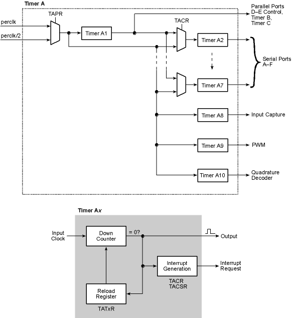
13.1 Overview
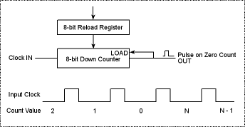
The Timer A peripheral consists of ten separate eight-bit countdown timers, A1–A10. Each counter counts down from a programmed time constant, which is automatically reloaded into the respective counter when the count reaches zero. For example, if the reload register contains 127, then 128 pulses enter on the left before a pulse exits on the right (see Figure 13-1). If the reload register contains zero, then each pulse on the left results in a pulse on the right, that is, there is division by one. The reload register can contain any number in the range from 0 to 255. The counter divides by (n + 1).
For Timers A1–A7 the terminal count condition is reported in a status register and can be programmed to generate an interrupt. Six of these seven timers (A2–A7) have the option of being cascaded from Timer A1, but the primary clock for all of the timers is the peripheral clock either directly or divided by 2 (the default). The output pulses are always one clock wide. Clocking of the timers takes place on the negative edge of this pulse. When the counter reaches zero, the reload register is loaded into the counter on the next input pulse instead of a count being performed.
Timers A2–A7 can be used to generate baud rates for Serial Ports A–F, or they can be used as general-purpose timers if the dedicated timers on the Rabbit 4000 serial ports are used. The three remaining timers (A8–A10) serve as prescalers for the input capture, PWM, and quadrature decoder peripherals respectively. The peripherals clocked by these timers can generate interrupts but the timers themselves cannot. Furthermore, these timers cannot be cascaded with Timer A1.
The individual Timer A capabilities are summarized in the table below. There is a bit in the control/status register to disable all ten timers globally.
There is one interrupt vector for Timer A and a common interrupt priority. A common status register (TACSR) has bits for timers A1–A7 that indicate if the output pulse for that timer has taken place since the last read of the status register. These bits are cleared when the status register is read. No bit will be lost. Either it will be read by the status register read or it will be set after the status register read is complete. If a bit is on and the corresponding interrupt is enabled, an interrupt will occur when priorities allow. However, a separate interrupt is not guaranteed for each bit with an enabled interrupt. If the bit is read in the status register, it is cleared and no further interrupt corresponding to that bit will be requested. It is possible that one bit will cause an interrupt, and then one or more additional bits will be set before the status register is read. After these bits are cleared, they cannot cause an interrupt. The proper rule to follow is for the interrupt routine to handle all bits that it sees set.
13.1.1 Block Diagram
13.1.2 Registers
13.2 Dependencies
13.2.1 I/O Pins
The output of Timer A does not come out directly on any of the I/O pins. It can be used to control when the output occurs on Parallel Ports D–E, and can affect the output times of Serial Ports A–F and the PWM.
13.2.2 Clocks
The timers in Timer A can be clocked by either perclk or perclk/2, as selected in TAPR. In addition, timers A2–A7 can be clocked by the output of timer A1 by selecting that option in TACSR.
13.2.3 Other Registers
GCSR
Select peripheral clock mode.
13.2.4 Interrupts
A Timer A interrupt can be generated whenever timers A1–A7 decrement to zero by enabling the appropriate bit in TACSR. The interrupt request is cleared when TACSR is read.
The Timer A interrupt vector is in the IIR at offset 0x0A0. It can be set as priority 1, 2, or 3 in TACR.
13.3 Operation
The following steps explain how to set up a Timer A timer.
- Select perclk as the Timer A input clock in TAPR (default is perclk/2).
- Select the source clocks for timers A2–A7 in TACR.
- Write the desired divider value to TATxR for all timers that will be used.
- Enable Timer A by writing a 1 to bit 0 of TACSR.
13.3.1 Handling Interrupts
The following steps explain how an interrupt is set up and used. Remember to set up the interrrupt vector before you enable the interrupts.
- Write the vector of the interrupt service routine to the internal interrupt table.
- Configure TACSR to select which timers will generate an interrupt.
- Configure TACR to select the interrupt priority (note that interrupts will be enabled once this value is set). This should be done last.
The interrupt request is cleared by reading from TACSR.
13.3.2 Example ISR
A sample interrupt handler is shown below.
timerA_isr::
   push af              ; save used registers
   ioi ld a, (TACSR)    ; clear the interrupt request and get status

   ; handle all interrupts flagged in TACSR here

   pop af               ; restore registers
   ipres
   ret
13.4 Register Descriptions
These bits are reserved and should be written with zero.
The main clock for Timer A is the peripheral clock (perclk).
The main clock for Timer A is the peripheral clock divided by two (perclk/2).
| Rabbit Semiconductor www.rabbit.com |