Rabbit 4000 Microprocessor
User's Manual
PREV INDEX NEXT


11. Parallel Port D

11.1 Overview

Parallel Port D is a byte-wide port with each bit programmable for data direction and drive level. These are simple inputs and outputs controlled and reported in the Port D Data Register (PDDR).

All of the Parallel Port D pins have alternate output functions, and all of them can be used as inputs to various on-chip peripherals.

When used as outputs, the Parallel Port D bits are buffered, with the data written to PDDR transferred to the output pins on a selected timing edge. Either the peripheral clock or the outputs of Timer A1, Timer B1, or Timer B2 can be used for this function, with each nibble of the port having a separate select field to control this timing. Each bit can either be programmed as open-drain or driven high and low.

Because of the buffered nature of Parallel Port D, using a read-modify-write type of operation can lead to old data being written to PDDR. To alleviate this potential problem, each bit of the port can be written individually using a separate address for each bit.

Parallel Port D acts as the upper byte of the data bus when the 16-bit mode is enabled; all other functionality of Parallel Port D will be automatically disabled when 16-bit mode is in effect.

Table 11-1. Parallel Port D Pin Alternate Output Functions

Pin Name

Alt Out 0

Alt Out 1

Alt Out 2

Alt Out 3

16-bit
Data Bus

PD7
IA7
I7
PWM3
SCLKC
D15
PD6
TXA
I6
PWM2
TXE
D14
PD5
IA6
I5
PWM1
RCLKE
D13
PD4
TXB
I4
PWM0
TCLKE
D12
PD3
IA7
I3
TIMER C3
SCLKD
D11
PD2
SCLKC
I2
TIMER C2
TXF
D10
PD1
IA6
I1
TIMER C1
RCLKF
D9
PD0
SCLKD
I0
TIMER C0
TCLKF
D8


Table 11-2. Parallel Port D Pin Alternate Input Functions

Pin Name

Input Capture

Serial Ports A–D

Serial Ports E–F

DMA

External Interrupts

Quad Decode

PD7
×
RXA
RXE


PD6


PD5
×
RXB
RCLKE


PD4


TCLKE


PD3
×
RXC
RXF
DREQ1

QRD2A
PD2

SCLKC

DREQ0

QRD2B
PD1
×
RXD
RCLKF

INT1
QRD1A
PD0

SCLKD
TCLKF

INT0
QRD1B


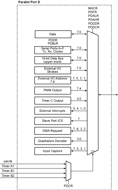
11.1.1 Block Diagram


11.1.2 Registers

Register Name

Mnemonic

I/O Address

R/W

Reset

Port D Data Register
PDDR
0x0060
R/W
xxxxxxxx
Port D Alternate Low Register
PDALR
0x0062
R/W
00000000
Port D Alternate High Register
PDAHR
0x0063
R/W
00000000
Port D Control Register
PDCR
0x0064
R/W
xx00xx00
Port D Function Register
PDFR
0x0065
R/W
xxxxxxxx
Port D Drive Control Register
PDDCR
0x0066
R/W
xxxxxxxx
Port D Data Direction Register
PDDDR
0x0067
R/W
00000000
Port D Bit 0 Register
PDB0R
0x0068
W
xxxxxxxx
Port D Bit 1 Register
PDB1R
0x0069
W
xxxxxxxx
Port D Bit 2 Register
PDB2R
0x006A
W
xxxxxxxx
Port D Bit 3 Register
PDB3R
0x006B
W
xxxxxxxx
Port D Bit 4 Register
PDB4R
0x006C
W
xxxxxxxx
Port D Bit 5 Register
PDB5R
0x006D
W
xxxxxxxx
Port D Bit 6 Register
PDB6R
0x006E
W
xxxxxxxx
Port D Bit 7 Register
PDB7R
0x006F
W
xxxxxxxx


11.2 Dependencies

11.2.1 I/O Pins

Parallel Port D uses pins PD0 through PD7. These pins can be used individually as data inputs or outputs; as serial port transmit and receive for Serial Ports A, B, E, and F; as clocks for Serial Ports C–F; as external I/O strobes; or as outputs for the PWM and Timer C peripherals. In addition, Parallel Port D acts as the upper byte of the data bus (D[15:8]) when 16-bit addressing is enabled. The input capture peripheral can also watch pins PD7, PD5, PD3, and PD1.

All pins are set as inputs on startup.

The individual bits can be set to be open-drain via PDDCR.

See the associated peripheral chapters for details on how they use Parallel Port D.

11.2.2 Clocks

All outputs on Parallel Port D are clocked by the peripheral clock unless changed in PDCR, where the option of updating the Parallel Port D pins can be synchronized to the output of Timer A1, Timer B1, or Timer B2.

11.2.3 Other Registers

Register

Function

SACR, SBCR, SCCR, SDCR, SECR, SFCR
Select a Parallel Port D pin as serial data (and optional clock) input.
ICS1R, ICS2R
Select a Parallel Port D pin as a start/stop condition input.
QDCR
Select a Parallel Port D pin as a decoder input.
I0CR, I1CR
Select a Parallel Port D pin as an external interrupt input.
DMR0CR, DMR1CR
Select a Parallel Port D pin as an external DMA request input.
MACR
Enable 16-bit data bus.


11.2.4 Interrupts

External interrupts can be accepted from pins PD1 or PD0; see Chapter 7 for more details.

11.3 Operation

The following steps must be taken before using Parallel Port D.

  1. Select the desired input/output direction for each pin via PDDDR.

  2. Select high/low or open-drain functionality for outputs via PDDCR.

  3. If an alternative peripheral output function is desired for a pin, select it by via PDALR or PDAHR and then enable it via PDFR. Refer to the appropriate peripheral chapter for further use of that pin.

  4. All these settings will be superseded if a 16-bit memory interface is selected since parallel port D is used for the upper half of the data bus in that mode.

Once Parallel Port D is set up, data can be read or written by accessing PDDR. The value of an output pin read in from PDDR will reflect its current output value, but any value written to an input pin will not appear until that pin becomes an output.

11.4 Register Descriptions

Parallel Port D Data Register (PDDR) (Address = 0x0060)

Bit(s)

Value

Description

7:0
Read
The current state of Parallel Port D pins PD7–PD0 is reported.
Write
The Parallel Port D buffer is written with this value for transfer to the Parallel Port D output register on the next rising edge of the peripheral clock.


Parallel Port D Alternate Low Register (PDALR) (Address = 0x0062)

Bit(s)

Value

Description

7:6
00
Parallel Port D bit 3 alternate output 0 (IA7).
01
Parallel Port D bit 3 alternate output 1 (I3).
10
Parallel Port D bit 3 alternate output 2 (TIMER C3).
11
Parallel Port D bit 3 alternate output 3 (SCLKD).
5:4
00
Parallel Port D bit 2 alternate output 0 (SCLKC).
01
Parallel Port D bit 2 alternate output 1 (I2).
10
Parallel Port D bit 2 alternate output 2 (TIMER C2).
11
Parallel Port D bit 2 alternate output 3 (TXF).
3:2
00
Parallel Port D bit 1 alternate output 0 (IA6).
01
Parallel Port D bit 1 alternate output 1 (I1).
10
Parallel Port D bit 1 alternate output 2 (TIMER C1).
11
Parallel Port D bit 1 alternate output 3 (RCLKF).
1:0
00
Parallel Port D bit 0 alternate output 0 (SCLKD).
01
Parallel Port D bit 0 alternate output 1 (I0).
10
Parallel Port D bit 0 alternate output 2 (TIMER C0).
11
Parallel Port D bit 0 alternate output 3 (TCLKF).


Parallel Port D Alternate High Register (PDAHR) (Address = 0x0063)

Bit(s)

Value

Description

7:6
00
Parallel Port D bit 7 alternate output 0 (IA7).
01
Parallel Port D bit 7 alternate output 1 (I7).
10
Parallel Port D bit 7 alternate output 2 (PWM3).
11
Parallel Port D bit 7 alternate output 3 (SCLKC).
5:4
00
Parallel Port D bit 6 alternate output 0 (TXA).
01
Parallel Port D bit 6 alternate output 1 (I6).
10
Parallel Port D bit 6 alternate output 2 (PWM2).
11
Parallel Port D bit 6 alternate output 3 (TXE).
3:2
00
Parallel Port D bit 5 alternate output 0 (IA6).
01
Parallel Port D bit 5 alternate output 1 (I5).
10
Parallel Port D bit 5 alternate output 2 (PWM1).
11
Parallel Port D bit 5 alternate output 3 (RCLKE).
1:0
00
Parallel Port D bit 4 alternate output 0 (TXB).
01
Parallel Port D bit 4 alternate output 1 (I4).
10
Parallel Port D bit 4 alternate output 2 (PWM0).
11
Parallel Port D bit 4 alternate output 3 (TCLKE).


Parallel Port D Control Register (PDCR) (Address = 0x0064)

Bit(s)

Value

Description

7:6
These bits are ignored and should be written with zero.
5:4
00
The upper nibble peripheral clock is the peripheral clock.
01
The upper nibble peripheral clock is the output of Timer A1.
10
The upper nibble peripheral clock is the output of Timer B1.
11
The upper nibble peripheral clock is the output of Timer B2.
3:2
These bits are ignored and should be written with zero.
1:0
00
The lower nibble peripheral clock is the peripheral clock.
01
The lower nibble peripheral clock is the output of Timer A1.
10
The lower nibble peripheral clock is the output of Timer B1.
11
The lower nibble peripheral clock is the output of Timer B2.


Parallel Port D Function Register (PDFR) (Address = 0x0065)

Bit(s)

Value

Description

7:0
0
The corresponding port bit functions normally.
1
The corresponding port bit carries its alternate signal as an output. See Table 11-1.


Parallel Port D Drive Control Register (PDDCR) (Address = 0x0066)

Bit(s)

Value

Description

7:0
0
The corresponding port bit, as an output, is driven high and low.
1
The corresponding port bit, as an output, is open-drain.


Parallel Port D Data Direction Register (PDDDR) (Address = 0x0067)

Bit(s)

Value

Description

7:0
0
The corresponding port bit is input.
1
The corresponding port bit is an output.


Parallel Port D Bit 0 Register (PDB0R) (Address = 0x0068)

Bit(s)

Value

Description

7:1
These bits are ignored.
0
Write
The port buffer (bit 0) is written with the value of this bit. The port buffer will be transferred to the port output register on the next rising edge of the peripheral clock


Parallel Port D Bit 1 Register (PDB1R) (Address = 0x0069)

Bit(s)

Value

Description

7:2,0
These bits are ignored.
1
Write
The port buffer (bit 1) is written with the value of this bit. The port buffer will be transferred to the port output register on the next rising edge of the peripheral clock


Parallel Port D Bit 2 Register (PDB2R) (Address = 0x006A)

Bit(s)

Value

Description

7:3,1:0
These bits are ignored.
2
Write
The port buffer (bit 2) is written with the value of this bit. The port buffer will be transferred to the port output register on the next rising edge of the peripheral clock


Parallel Port D Bit 3 Register (PDB3R) (Address = 0x006B)

Bit(s)

Value

Description

7:4,2:0
These bits are ignored.
3
Write
The port buffer (bit 3) is written with the value of this bit. The port buffer will be transferred to the port output register on the next rising edge of the peripheral clock


Parallel Port D Bit 4 Register (PDB4R) (Address = 0x006C)

Bit(s)

Value

Description

7:5,3:0
These bits are ignored.
4
Write
The port buffer (bit 4) is written with the value of this bit. The port buffer will be transferred to the port output register on the next rising edge of the peripheral clock


Parallel Port D Bit 5 Register (PDB5R) (Address = 0x006D)

Bit(s)

Value

Description

7:6,4:0
These bits are ignored.
5
Write
The port buffer (bit 5) is written with the value of this bit. The port buffer will be transferred to the port output register on the next rising edge of the peripheral clock


Parallel Port D Bit 6 Register (PDB6R) (Address = 0x006E)

Bit(s)

Value

Description

7,5:0
These bits are ignored.
6
Write
The port buffer (bit 6) is written with the value of this bit. The port buffer will be transferred to the port output register on the next rising edge of the peripheral clock


Parallel Port D Bit 7 Register (PDB7R) (Address = 0x006F)

Bit(s)

Value

Description

6:0
These bits are ignored.
7
Write
The port buffer (bit 7) is written with the value of this bit. The port buffer will be transferred to the port output register on the next rising edge of the peripheral clock


Rabbit Semiconductor
www.rabbit.com
PREV INDEX NEXT