User's Manual
|
|
| Rabbit 4000 Microprocessor User's Manual |
|
19. DMA Channels
19.1 Overview
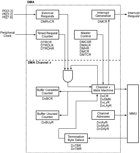
There are eight independent DMA channels on the Rabbit 4000. All eight channels are identical, and are capable of transferring data to or from memory, external I/O, or internal I/O. The priority between the channels can be either fixed or rotating, and the DMA use of the bus can be limited to guarantee interrupt latency or CPU throughput. The DMA channels are capable of special handling for the last byte of data when sending data to selected internal I/O addresses (such as the HDLC serial ports or to the Ethernet peripheral), and can also transfer end-of-frame status after transferring data from selected internal I/O addresses.
The DMA channels can watch the data being transferred and can terminate a transfer when a particular byte is matched. A mask is available for the byte match to allow termination only on particular bit settings in the data instead of an exact byte match.
Memory-to-memory transfers proceed at the maximum transfer rate unless they are gated by an external request signal or the internal timed request. Transfers to or from a number of internal I/O addresses are controlled by transfer request signals. These transfer request signals are connected automatically as a function of the internal I/O address loaded into the DMA channel. Note that if both the source and the destination are internal I/O, the source transfer request is used by the DMA channel.
The DMA channels are inherently byte-oriented, so while DMA transfers can be done from a 16-bit memory, DMA transfers to a 16-bit memory can only be done if the 16-bit memory is set up to allow byte writes. See Chapter 5 for more information.
There are two inputs available for requests linked to external I/O devices. These two external requests may be assigned to any DMA channel. These requests may also be used by a channel that has an internal I/O as a destination. In this case, the external request acts as a "flow control" signal for the DMA transfers because the external request is "ANDed" with the automatically connected internal request.
To facilitate periodic DMA transfers, there is also an internal timed request. This request is generated from a programmable 16-bit counter and may be assigned to any DMA channel. As in the case of the external requests, this request is "ANDed" with any internal or external request that is also assigned to that DMA channel. This periodic request can be programmed to transfer one byte or an entire buffer. The single-byte option is useful for driving an output port to create a sampled waveform, while the entire-buffer option can be used, for example, to send precisely timed serial messages over a serial port.
The DMA operation is controlled by memory structures called buffer descriptors. The current buffer descriptor resides in the registers of the DMA channel, but may have been placed there either by the processor or loaded directly by the DMA channel itself. Buffer descriptors may be used singly, to transfer one block of data, or they may be linked together for "scatter-gather" operation. Each DMA channel also contains an "initial address" that points to the first buffer descriptor in memory and allows the DMA channel to rewind itself automatically in the case of a transmit retry by the network port. Each buffer descriptor contains a control byte, a byte count for the data, a source address, a destination address, and an optional link address. In addition, each DMA channel retains a count of the number of bytes remaining in the buffer to allow software to determine the amount of valid data in a buffer that are terminated early by the source of the data.
A buffer descriptor in memory consists of either 12 or 16 consecutive bytes organized as shown in Table 19-1. The DMA channel uses the information in the control byte to determine the length of the buffer descriptor as well as which information to fetch from the buffer descriptor. If no link address field is present, the buffer descriptor is only 12 bytes long. A memory address for either source or destination causes the DMA channel to fetch three bytes from the corresponding field in the buffer descriptor. An internal I/O or external I/O address for either source or destination causes the DMA channel to fetch two bytes from the corresponding field in the buffer descriptor.
DMA memory addresses are always physical addresses, and are never translated by the MMU. All DMA memory addresses use the memory control signals, wait states, and flipped bits as selected in the Master Memory Bank Control registers. All DMA external I/O addresses use the I/O control signals and wait states as selected in the external I/O registers.
The first byte in the first buffer descriptor (the byte pointed to by the initial address) is reserved for status information when transferring data from an internal serial or network device. This automatic status transfer means that the processor does not need to service any interrupts from a serial or network receiver except in the case of an error condition.
When transferring data to an internal HDLC serial or network transmitter, the last byte of the last buffer will automatically be written to a special destination address to tag the data as the last in the frame, without processor intervention. However, this function is not available in the case where the buffer contains only one byte of data. If this case should occur, the buffer descriptor must contain the special destination address.
All the DMA channels request interrupts at the same priority level, which is set by a field in the DMA Master Control Register, but each DMA channel has its own interrupt vector location. This speeds up interrupt processing for the DMA interrupts by eliminating the need to resolve which DMA channel is actually requesting an interrupt.
DMA transfers may be programmed to occur at any priority level. If the programmed level is greater than or equal to the current CPU operating level, DMA transfers will occur on demand. When the CPU operating level is greater than the programmed DMA operating level, no DMA transfers can occur. This allows interrupt services routines, or other critical code, to run with a guarantee that there will be no DMA activity during execution. Note that a simultaneous interrupt request and DMA transfer request will be resolved in favor of the DMA transfer request.
The DMA and Ethernet peripherals were optimized to work together; if the Rabbit 4000's built-in Ethernet peripheral is used it is expected that two DMA channels will be dedicated for that purpose.
19.1.1 Block Diagram
19.1.2 Registers
NOTE The y in "DMA y ..." expresses the DMA channel number (0–7). 19.2 Dependencies
19.2.1 I/O Pins
External DMA Request 0 can be enabled from pins PD2, PE2, or PE6. External DMA Request 1 can be enabled from pins PD3, PE3, or PE7.
The DMA can use either the memory management unit or the auxiliary I/O bus to perform its transfers, and so will use the appropriate pins for each operation.
19.2.2 Clocks
The DMA peripheral uses the peripheral clock for all operations. If the timed request option is enabled, then the 16-bit timed request counter will be clocked by the peripheral clock and will provide a DMA request each time it counts down to zero.
19.2.3 Interrupts
Each DMA channel has its own dedicated interrupt that can occur at the end of any DMA transfer, as specified in DyCR (normally loaded from the buffer descriptor). The interrupt request is automatically cleared when the interrupt is handled.
The DMA interrupt vectors are in the EIR starting at offset 0x080 for DMA Channel 0 and ending at offset 0x0F0 for DMA Channel 7. They can be set as Priority 1, 2, or 3.
19.3 Operation
It is possible to set up and start a DMA operation by writing directly to all the relevant address, length, and control registers, but it is expected that the typical operation would be to create a buffer descriptor in memory, write the address of that descriptor to the initial address registers (DyIAnR), and use a write to DMALR to auto-load the values from memory into the registers and start the transfer. The DMA transfer will then continue reading buffer descriptors until a buffer-marked halt is completed.
The descriptor can be either 12 or 16 bytes in length; a bit in the channel control byte (which corresponds to DyCR) selects whether the link address is present or not. The processor skips the read of those bytes if a 12-byte descriptor is selected, and always skips the reads of the bytes marked "not used."
Table 19-1. DMA Buffer Descriptor Bytes 0–3
Bytes 4–7
Bytes 8–11
Bytes 12–15
It is possible to abort a DMA transfer by writing the appropriate bit to the halt register, DMHR. It is also possible to restart a DMA transfer using the already-loaded register values by writing to DMCSR.
The following steps explain how to set up a DMA channel.
- Select the DMA transfer and interrupt priorities by writing to DMCR.
- Select the DMA channel priority, maximum bytes per burst, and minimum clocks between bursts by writing to DMTCR.
- Write the interrupt vector for the interrupt service routine to the external interrupt table.
- Enable an external request line by writing to DMR0CR or DMR1CR. Make sure that the pin selected is set up as an input. Note that this enable will be logical-ANDed to any internal DMA enables if the DMA transfer is to/from an internal peripheral.
- Enable the internal-timed transfer request by writing to DTRCR. Select the divider value by writing to DTRDLR and DTRDHR. Note that this enable will be logical-ANDed to any internal DMA enables if the DMA transfer is to/from an internal peripheral.
- Select a byte to terminate the transfer on by writing to the appropriate DyTBR and DyTMR registers.
- The desired control, length, and address registers should be written to a buffer descriptor (or descriptors) in memory if not done already.
- The initial address registers (DyIAnR) should be loaded with the physical address of the first buffer descriptor.
- The buffer descriptor can be loaded and the DMA transfer started by writing to the appropriate bit of DMALR.
19.3.1 Handling Interrupts
The DMA interrupt request is cleared automatically when the interrupt is handled. A DMA interrupt will occur at the end of a transfer for any buffer descriptor that has bit 4 of DyCR set.
19.3.2 Example ISR
A sample interrupt handler is shown below.
dma_isr::
   push af
   ; do something with the data in the current buffer
   ; the interrupt request is automatically cleared

   pop af
   ipres
   ret
19.3.3 DMA Priority with the Processor
Since the Rabbit 4000 DMA uses the memory management unit to perform transfers, normal code execution cannot occur while the DMA is active. This includes handling interrupts, so it is important to limit the amount of time that the DMA can operate.
This is handled in several ways. First of all, the DMA transfers can be set to take place whenever the processor is operating at one of the four priority levels, 0–3 (note that there is a single priority level for all DMA transfers). Setting an interrupt priority to something greater than the DMA transfer priority will ensure that no DMA activity occurs during that interrupt handler. Note that when both an interrupt and a DMA transfer are pending, the DMA transfer will be selected for execution first (provided its priority is equal or greater than the current processor priority level).
Table 19-2. DMA Transfer Priority
When a DMA transfer is occurring, normal code execution will not occur until the transfer is completed. To prevent DMA transfers from excessively blocking interrupts or otherwise interfering with normal code execution, two options can be set in DMTCR. First, the maximum limit of a DMA transfer can be set from 1 to 64 bytes, which sets an upper limit on interrupt latency arising from a DMA transfer. Second, the minimum number of clocks before the DMA can be active again can be set from 12 to 512 clocks, guaranteeing processing time for the application.
The values providing roughly equal access to the memory bus for both the processor and the DMA is eight bytes per burst and 64 clocks between bursts.
When starting up, the DMA requires several cycles of overhead. This overhead comes about because the DMA actually uses part of the processor to perform the data transfers, and consists of one instruction fetch time plus three clock cycles. The byte fetched during the instruction fetch time is discarded, and will be refetched at the completion of the DMA burst. At the end of the DMA burst, two clock cycles are required before this first instruction fetch starts. An individual DMA channel transfers data without any overhead between bytes, but there is always one clock cycle of dead time when switching between DMA channels. Table 19-3 shows the number of clock cycles required per burst, assuming a single DMA channel transfer and no wait states.
Table 19-3. Maximum DMA Transfer Rates
The total number of clocks listed in Table 19-3 is related to the number of bystes per burst by the following formula.
19.3.4 DMA Channel Priority
It is possible to control the priority between separate DMA channels. There are three channel-priority options in the Rabbit 4000. The first is fixed priority after every byte where the priority of each channel is equal to its number, i.e., if both DMA Channels 3 and 4 have a pending transfer request, DMA Channel 4 will always be enabled first. If at any point a channel with higher priority than the one currently transferring has a DMA request pending, the current transfer will be terminated and the new channel's transfer will start. With this setting, DMA Channel 7 will always have priority over all other channels, and DMA Channel 0 will transfer only if no other channels have pending requests.
The other two settings rotate the priority between channels as shown in Table 19-4; after the seventh rotation, the priority sequence restarts at the top of the table. One option is to rotate priority after every byte analogous to the fixed-priority setting. The priority list is updated after each byte transferred, and if a higher priority channel has a pending request the current transfer will be terminated and the new channel transfer will start. The other option is to rotate after every burst; this will guarantee that reasonable amounts of data are transferred by each channel before a switchover occurs.
Table 19-4. Rotating DMA Channel Priority
19.3.5 Buffer Descriptor Modes
Flags in the control byte of a buffer descriptor (which gets loaded into DyCR) describe whether to halt on completion of the transfer (or load another descriptor) and whether the next descriptor is adjacent in memory (which implies that the current descriptor is only 12 bytes long) or located at the link address. Each descriptor can also be set to generate an interrupt on completion of the transfer. By using these options in various ways, the Rabbit 4000 DMA can be operated in a number of conventional DMA modes.
The most common options are described here; others are certainly possible by different use of the available linking methods.
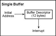
19.3.5.1 Single Buffer
In the simplest mode, a single descriptor is set to halt and interrupt on completion.
19.3.5.2 Buffer Array
In this mode, an array of 12-byte descriptors is set up adjacent in memory; only the last buffer is set to halt on completion. The last buffer is also typically set to interrupt on completion, but other buffer descriptors in the array can also generate interrupts.
The advantage of the buffer array is that its descriptors require less memory than a full 16-byte descriptor.
The simplest version of the buffer array is a double buffer, which is frequently used to provide a reserve buffer in case the application is slow in handling the first buffer once received (in this case, both buffers are enabled to interrupt on completion).
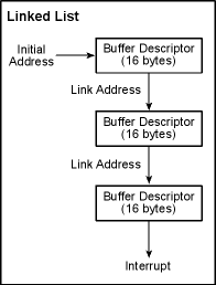
19.3.5.3 Linked List
A linked list is similar to a buffer array, except that 16-byte descriptors are used and the descriptors are not necessarily adjacent in memory. The advantage of this mode is the ability to spread descriptors.
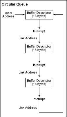
19.3.5.4 Circular Queue
A circular queue is a buffer array or linked list where the final buffer is linked back to the first buffer in the sequence. This method allows for continuous reception of transfers without having to reload the initial address for the DMA buffer descriptor sequence.
The "ping-pong buffer," where there are only two buffers, is the simplest version of a circular queue. The application can operate on one buffer while the other buffer is being loaded.
19.3.5.5 Linked Array
The linked array is simply a linked list of buffer arrays, where the last buffer in each array is linked to the first buffer in the next array (which can be located anywhere in memory). This method could be useful where a message is broken down into separate transfers, but entire messages could be scattered/gathered from anywhere in memory.
19.3.6 DMA with Peripherals
When the DMA is directed towards an internal I/O address, the DMA transfer request signals will be connected as appropriate for that peripheral. For example, when a DMA transfer is performed to Serial Port D's data register, the transfer request will be enabled whenever the serial port transmit buffer is empty, and will be disabled whenever it is not.
19.3.6.1 DMA with HDLC Serial Ports
The HDLC serial ports receive special handing by the DMA. When the DMA destination is Serial Port E's or Serial Port F's data register (SxDR), the final byte of the transfer will be written to the appropriate last data register (SxLDR) as required to complete an HDLC packet and append the CRC value. In addition, the value in the appropriate status register (SxSR) will be written to the status byte in the buffer descriptor pointed to by the initial address registers (not necessarily the buffer descriptor that is currently being used). These features allow an application to automatically send and receive packets via DMA, only requiring direct handling of a packet when an error occurs.
19.3.6.2 DMA with Ethernet
The Ethernet network peripheral also receives special handing by the DMA. When the DMA destination is the network data register (NADR), the final byte of the transfer will be written to the last data register (NALDR) as required to complete an Ethernet packet and append the CRC value. In addition, the value in the network status register (NASR) will be written to the status byte in the buffer descriptor pointed to by the initial address registers (not necessarily the buffer descriptor that is currently being used). These features allow the processor to only handle interrupts when an error occurs.
19.3.6.3 DMA with PWM and Timer C
The PWM and Timer C peripherals have special support for DMA; the block access and pointer registers in each of these peripherals provide a means for the DMA to update the settings of these peripherals at some desired rate. This allows complex PWM waveforms to be generated by using the DMA timed request to update the PWM duty cycles at regular intervals.
19.3.7 DMA Bug Workarounds (Appendix B.2)
19.3.7.1 DMA/HDLC/Ethernet Interaction
A specific bug can manifest itself when the following conditions are present.
· The HDLC or Ethernet peripherals are being fed bytes for transmit via DMA. · The current DMA buffer has been marked with "special treatment for last byte." · The buffer has not been marked as "final buffer." · The DMA fills the transmit FIFO with the next-to-last byte of the buffer and then either switches to another channel or releases the bus. · The DMA then returns to the channel before the transmitter has had a chance to transmit a single byte, freeing space in the transmit FIFO. When all these conditions occur, the DMA will overwrite the next-to-last byte in the transmit FIFO, and that particular byte will never be transmitted.
There are several ways to avoid this bug.
· Always mark the buffer that contains the end-of-frame byte as the final buffer, and restart the DMA once that buffer has been transmitted. · Make sure that the DMA will not return to this channel before the transmitter has sent one byte from the transmit FIFO. · Place the end-of-frame byte in a separate DMA buffer. The Ethernet driver provided by Rabbit Semiconductor in Dynamic C is written so that this bug never occurs.
19.3.8 DMA/Block Copy Interaction
When a DMA transfer occurs during a block copy instruction (LDIR, LDDR, COPY, COPYR, UMA, or UMS) while executing code out of 16-bit memory with the "advanced 16-bit mode" enabled, the code prefetch queue and program counter will become out-of-synch. This means that one or two incorrect bytes (depending on the 16-bit alignment of the instruction) are reloaded and presented to the processor as instructions when execution is "rewound" after the DMA transfer. The result of this mismatch is that the block copy instruction does not complete.
The only way to prevent this from occurring is to prevent DMA transfers during block copy instructions, either by disabling the DMA or by increasing the processor priority above the priority of the DMA transfer.
There is a workaround. The processor's BC register is used as a program counter by the block copy instructions, and will be nonzero if the block copy instruction did not complete. By checking the value of BC and jumping back to the block copy instruction if it is nonzero, the block copy instruction is restarted with all the current register values (source and destination pointers) and will continue where it left off. Rabbit Semiconductor's Dynamic C compiler automatically includes this wrapper code whenever it identifies a block copy instruction.
19.3.9 Single-Byte DMA Requests to internal I/O Registers
When timed or external DMA requests are enabled and set to transfer a single byte at a time to an internal I/O register, two bytes will actually be transferred. The simplest workaround is to double each data byte in the buffer; two bytes will be transmitted, but they will be identical, so the actual I/O register setting will not change.
19.4 Register Descriptions
No effect of the corresponding DMA channel.
Halt the corresponding DMA channel. The DMA registers retain the current state, and the DMA can be restarted using the DMCSR.
The eight LSBs of the limit value for the DMA timed request timer are stored.
The eight MSBs of the limit value for the DMA timed request timer are stored.
Byte value that, if matched, will terminate a buffer.
Bits 15:8 of the buffer unused-length value are stored in this register.
Bits 7:0 of the initial address are stored in this register.
Bits 15:8 of the initial address are stored in this register.
Bits 23:16 of the initial address are stored in this register.
Bits 7:0 of the buffer length value are stored in this register. The DMA does a transfer followed by a decrement of this register, so an initial value of 0x0000 will result in a 65536-byte transfer.
Bits 15:8 of the buffer length value are stored in this register.
Bits 7:0 of the source address are stored in this register.
Bits 15:8 of the source address are stored in this register.
Bits 23:16 of the source address are stored in this register.
Bits 7:0 of the destination address are stored in this register.
Bits 15:8 of the destination address are stored in this register.
Bits 23:16 of the destination address are stored in this register.
Bits 7:0 of the link address are stored in this register.
Bits 15:8 of the link address are stored in this register.
Bits 23:16 of the link address are stored in this register.
| Rabbit Semiconductor www.rabbit.com |