User's Manual
|
|
| Rabbit 4000 Microprocessor User's Manual |
|
18. Slave Port
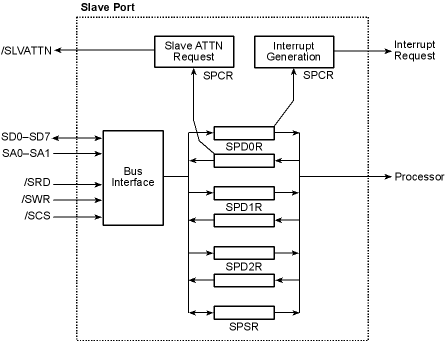
18.1 Overview
The slave port is a parallel communication port that can be used to communicate with an external master device. The slave port consists of three data input and data output registers, and a status register.
The data input registers are written by the master (the external device) and are read by the processor. The data output registers are written by the processor and are read by the master. Note that the data registers are named from the point of view of the processor. The slave device can only read the data input registers and write to the data output registers. Similarly, the master device can only read the data input registers and write the data output registers. Both devices can read and write to the status register.
The status register contains the interrupt status bits and a status flag corresponding to each data input or data output register to indicate the empty or full status of the data register. Data registers are marked full when written by the source side of the interface, and are marked empty when read by the destination side of the interface.
The hardware interface to the external master consists of an 8-bit bidirectional data bus with a read strobe, write strobe, and chip select. There are two address lines that select one of the three data registers or the status register.
Table 18-1. Slave Port Addresses
A slave attention signal is asserted when the processor writes to one of the slave port data registers (SPD0R), and can be deasserted by the master by performing a dummy write to the status register. This signal can be used to interrupt the master to indicate that the master needs to read data from the slave.
The slave port interrupt is asserted when the master writes to SPD0R. The processor clears this interrupt condition by writing to the status register.
The slave port can be used to bootstrap the processor by setting the SMODE pins appropriately. See Chapter 3 for more information on this mode.
18.1.1 Block Diagram
18.1.2 Registers
Slave Port Data 0 Register
Slave Port Data 1 Register
Slave Port Data 2 Register
Slave Port Status Register
Slave Port Control Register
18.2 Dependencies
18.2.1 I/O Pins
When the slave port is enabled by writing to SPCR, the following pins are enabled for slave port mode. Note that enabling the slave port mode will override any general-purpose I/O or auxiliary I/O bus settings for these pins; when the slave port is enabled they will perform slave port functionality.
Table 18-2. Slave Port Pin Functionality Slave data bus
Slave interrupt request (output)
Slave chip select
Slave address bus
Slave port read strobe
Slave port write strobe
Alternate slave chip select
18.2.2 Clocks
All slave port operations are based on the processor clock.
18.2.3 Interrupts
A slave port interrupt occurs on the slave device whenever the master writes to SPD0R. The /SLVATTN pin is asserted whenever the slave device writes to SPD0R. Either if these conditions is cleared when either the master or slave reads or writes any of the slave port registers.
The slave port interrupt vector is in the IIR at offset 0x080. It can be set as Priority 1, 2, or 3 by writing to SPCR.
18.3 Operation
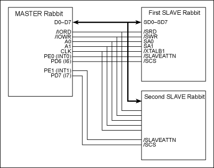
Figure 18-1 shows a typical slave port connection between a Rabbit processor as the master and two slaves.
These connections are summarized in Table 18-3.
Note that the slave port on the master Rabbit processor is not used; the master uses the data bus to send and receive data to the slave port data registers on the slave devices.
In this setup, pins PD6 and PD7 are set up as I/O strobe chip selects for the two slave devices, and PE0 and PE1 are used as external interrupt inputs to monitor the /SLVATTN signals from the slaves.
In this setup, the slave port is used as follows:
- The slave responds to the interrupt and reads the slave port data registers.
- When the slave wishes to send data to the master, it writes the slave port data registers, writing SPD0R last, which enables the /SLVATTN signal.
- When the master detects the change on /SLVATTN, it reads the slave port data registers.
18.3.1 Master Setup
- Enable the I/O strobes on PD6 and PD7 by writing to the appropriate Parallel Port D pin and external I/O registers.
- Enable the external interrupts on PE0 and PE1 by writing to the appropriate external interrupt registers.
18.3.2 Slave Setup
- Write the vector to the interrupt service routine to the internal interrupt table.
- Configure SPCR to select the interrupt priority (note that interrupts will be enabled once this value is set).
18.3.3 Master/Slave Communication
- The master writes data to the appropriate external I/O address on the data bus for the slave device and register desired. For example, in the setup described here, the master would write to register SPD2R on the first slave by writing to the address 0xC002 (0xC000 for the I6 strobe, and 0x0002 for SPD2R on that slave).
- If the master is writing multiple bytes, it should write to SPD0R last since that will trigger an interrupt on the slave device. If only one byte is being sent, it should be written to SPD0R.
- The slave responds to the interrupt, reading the data from the slave port data registers.
18.3.4 Slave/Master Communication
- The slave writes data to the appropriate slave port data register. If it is writing multiple bytes, SPD0R should be written last, which enables the /SLVATTN line.
- The master receives an external interrupt from the /SLVATTN line, and reads the data out of the slave port data registers via external I/O reads on the data bus.
18.3.5 Handling Interrupts
The interrupt request on the slave is cleared by either the master or the slave accessing one of the slave port registers. To clear the interrupt without affecting the register values, a dummy write can be made to SPSR.
18.3.6 Example ISR
A sample interrupt handler is shown below.
slave_isr::
   push af             ; save used registers

   ; read the data sent by the master
   ioi ld a, (SPD2R)
   ld (to_slv_d2), a
   ioi ld a, (SPD1R)
   ld (to_slv_d1), a
   ioi ld a, (SPD0R)
   ld (to_slv_d0), a

   ; if a response is required, perform it here
   ld a, (to_mas_d2)
   ioi ld (SPD2R), a
   ld a, (to_mas_d1)
   ioi ld (SPD1R), a
   ld a, (to_mas_d0)
   ioi ld (SPD0R), a   ; this write asserts /SLVATTN

   ; the interrupt request is cleared by any read/write of the registers

   pop af              ; restore used registers
   ipres
   ret
18.3.7 Other Configurations
There are other slave port configurations possible:
- The master could use the auxiliary I/O bus instead of the memory bus.
- All devices could poll the slave port status register to determine when data is present instead of relying on interrupts.
- The master could write to SPD0R, triggering an interrupt on the slave. The slave could then simply write a response into SPD0R, which the master detects by polling SPSR. This configuration is useful when fewer signals are desired, or the master device has no external interrupts available.
If polling is to be used, it is important to note that not all bits in the status register may be updated at once; it is possible to read a transitional value as the register updates. To guarantee a proper polling read, the status register should be read twice; when the same value is read both times the value is correct.
Similarly, it is possible to receive a scrambled value from a data register if it is read while being written. The protocol used should take account of this and prevent it from occurring (the protocol described above guarantees this will not occur).
18.3.8 Timing Diagrams
Figure 18-2 shows the sequence of events when the master reads/writes the slave port registers.
The following table explains the parameters used in Figure 18-2.
18.4 Register Descriptions
The corresponding byte of the slave port is read.
The corresponding byte of the slave port is written.
| Rabbit Semiconductor www.rabbit.com |