User's Manual
|
|
| Rabbit 4000 Microprocessor User's Manual |
|
17. Serial Ports E – F
17.1 Overview
Serial Ports E and F are identical to each other, and their asynchronous operation is identical to that of Serial Ports A – D except for the source of the data clock, the buffer sizes, and the transmit, receive, and clock pins. Each serial port can be used in the asynchronous or the HDLC mode with an internal or external clock.
In the asynchronous mode, either 7 or 8 data bits can be transferred, and both a parity bit and/or an additional address (0) or long stop (1) bit can be appended as well. Parity and the address/long stop bits are also detected when they are received. The asynchronous mode is full-duplex.
The transmit and receive buffers of Serial Ports E and F have 4 bytes each; this reduces the interrupt overhead requirements. A serial port interrupt is generated whenever at least one byte is available in the receive buffer or whenever a byte is shifted out of the transmit buffer. The byte is available in the buffer after the final bit is sampled.
The status of each serial port is available in the Serial Port Status Registers (SxSR), and contains information on whether a received byte is available, the receive buffer was overrun, a parity error was received, and the transmit buffer is empty or busy sending a byte. The status is updated when the final bit of a received byte is sampled, or when the final bit of a transmitted byte is sent out.
Serial Ports E and F support the HDLC mode with either an internal or an external clock; separate pins may be used for the transmit and receive clocks, or the transmit and receive clocks may be combined onto a single pin. The HDLC packet flag encapsulation, flag escapes, and CRC calculation and check are handled automatically by the processor. The serial port can detect end-of-frame, short-frame, and CRC errors. Interrupts are generated by the reception of an end-of-frame, at the end of a transmission of a CRC, by an abort sequence, or by a closing flag. Transmit and receive operations are essentially automatic.
The standard CRC-CCITT polynomial (x16 + x12 + x5 + 1) is implemented for the CRC, with the generator and checker preset to all ones.
It is possible to send packets with or without a CRC appended. It is also possible to select whether an abort or flag will be transmitted if the transmitter underflows. A packet under transition can be aborted and the abort pattern sent. The idle condition of the line can be flags or all ones.
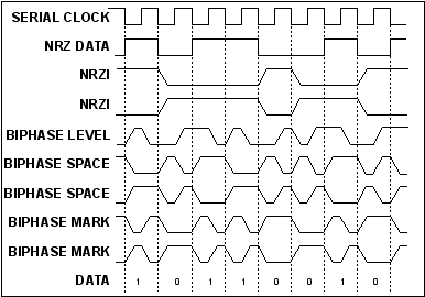
Several types of data encoding are available in HDLC mode: NRZ, NRZI, biphase-level (Manchester), biphase-space (FM0), and biphase-mark (FM1). IrDA-compliant RZI encoding is also available in HDLC mode; it reduces the bit widths to ¼ the normal width, which allows the serial-port signal to be connected directly to an IrDA transceiver.
If an internal clock is selected, the serial port data clocks can be generated from the appropriate 8-bit timer (Timer A2 for Serial Port E and Timer A3 for Serial Port F) or from a dedicated 15-bit divider. In HDLC mode, the byte data rate is equal to the data clock rate divided by 16.
When using an external clock, a 1× (same speed as the data rate) clock is supported. In this case, the maximum data rate is 1/6 of the peripheral clock rate. The receive clock is generated from the transitions in the data stream via a digital phase-locked loop (DPLL). The timing of this synchronization is adjusted with each incoming transition, allowing for tracking if the two external clocks differ slightly in frequency. For more on the clock synchronization and data encoding, see Section 17.3.3.
17.1.1 Block Diagram
17.1.2 Registers
17.2 Dependencies
17.2.1 I/O Pins
Serial Port E can transmit on parallel port pins PC6, PD6, or PE6, and can receive on pins PC7, PD7, or PE7. If the HDLC mode is enabled, the transmit serial clock is either transmitted or received on PC4, PD4, or PE4, while the receive serial clock is either transmitted or received on PC5, PD5, or PE5.
Serial Port F can transmit on parallel port pins PC2, PD2, or PE2, and can receive on pins PC3, PD3, or PE3. If the HDLC mode is enabled, the transmit serial clock is either transmitted or received on PC0, PD0, or PE0, while the receive serial clock is either transmitted or received on PC1, PD1, or PE1.
Table 17-1. Serial Ports E and F Pin Usage 17.2.2 Clocks
The data clocks for Serial Ports E – F are based on the peripheral clock and divided by either a Timer A divider or a dedicated 15-bit divider. In either case, the overall clock divider will be the value in the appropriate register plus one.
17.2.3 Other Registers
TAT2R
Time constant for Serial Port E
TAT3R
Time constant for Serial Port F
PCFR, PCAHR, PCALR
PDFR, PDAHR, PDALR
PEFR, PEAHR, PEALR
Alternate port output selection
17.2.4 Interrupts
In the asynchronous mode, a serial port interrupt can be generated whenever a byte is available in the receive buffer or when a byte is finished being transmitted out of the transmit buffer. In the HDLC mode, interrupts are also generated by the reception of an end-of-frame (with abort, valid CRC, or CRC error), at the end of a transmission of a CRC, by an abort sequence, or by a closing flag.
The serial port interrupt vectors are located in the IIR as follows.
Each of them can be set as Priority 1, 2, or 3 in SxCR, where x is E – F for the two serial ports.
17.3 Operation
17.3.1 Asynchronous Mode
The steps to set up Serial Ports E – F for asynchronous operation are identical to those described in Section 16.3.1 to set up Serial Ports A – D.
17.3.2 HDLC Mode
The following steps explain how to set up Serial Ports E – F for the HDLC mode. When the internal clock is selected, the Rabbit 4000 is in control of all transmit and receive operations, so an interrupt is not required. When an external clock is selected, operations can be handled by either polling the status byte or by a serial port interrupt; the performance will be better with an interrupt.
- Write the interrupt vector for the interrupt service routine to the internal interrupt table.
- Set up the desired data transmit and clock pins by writing to the appropriate parallel port function register (PxFR) and alternate output register (PxALR or PxAHR).
- Select the appropriate mode by writing to SxCR (receive input port and clock source). Also select the interrupt priority.
- Select additional options by writing to SxER (data encoding, idle line condition, underrun behavior, and combined or separate clocks).
- Write the desired divider value to TATxR for the appropriate serial port, or else write a divider to the dedicated 15-bit divider in SxDLR and SxDHR. If the dedicated divider is to be used, write a 1 to the most-significant bit of SxDHR to enable it. In either case, the overall clock divider will be the value in the appropriate register plus one.
- To start transmission of a packet, write the first byte to SxDR. If internal clock is selected, the transmission will begin immediately; if an external clock is selected the transmission will begin when the clock is detected.
- Continue writing bytes when space is available in the transmit buffer until the final byte of the packet. If a CRC is to be appended to the packet, write the final byte to SxAR. If no CRC is required, write the final byte to SxLR and just a closing flag will be appended. If it is desirable to abort the current packet, write 11 to bits 6–7 of SxCR, and an abort pattern will be transmitted.
- The receiver will be synchronized on flag bytes and will reset the CRC. By monitoring the received bytes, decisions can be made about the incoming packet; if it is not desired (i.e., it is not addressed to this device), writing a 01 to bits 6–7 of SxCR will force the receiver back into the flag search mode.
A sample HDLC interrupt handler is shown below for Serial Port E.
hdlc_sere_isr::
   push af
   ioi ld a, (SESR)    ; get status
   bit a,7               ; check if byte ready in RX buffer
   push af             ; save status for next check
   jr  z, check_for_tx
rx_ready:

   ; check status byte in A for abort or invalid CRC flags

   ioi ld a, (SADR)    ; read byte and clear interrupt

   ; store byte in A here

check_for_tx:
   pop af
   bit a,3               ; check if TX buffer was emptied
   jr nz, done

   ; check status byte in A for transmit finish reason (CRC, abort, etc.)

   ; get next byte to be transmitted into A here; if it is the last
   ;   byte of the packet, load it into SEAR or SELR instead

   ioi ld (SEDR), a    ; load next byte into buffer and clear interrupt
done:
   pop af
   ipres
   ret
17.3.3 More on Clock Synchronization and Data Encoding
The transmitter is not capable of sending an arbitrary number of bits, but only a multiple of bytes. However, the receiver can receive frames of any bit length. If the last "byte" in the frame is not eight bits, the receiver sets a status flag that is buffered along with this last byte. Software can then use the table below to determine the number of valid data bits in this last "byte." Note that the receiver transfers all bits between the opening and closing flags, except for the inserted zeros, to the receiver data buffer.
Several types of data encoding are available in the HDLC mode. In addition to the normal NRZ, they are NRZI, biphase-level (Manchester), biphase-space (FM0), and biphase-mark (FM1). Examples of these encodings are shown below. Note that the signal level does not convey information in NRZI, biphase-space, and biphase-mark. Instead it is the placement of the transitions that determine the data. In biphase-level it is the polarity of the transition that determines the data.
In the HDLC mode the internal clock comes from the output of Timer A2/Timer A3 or the dedicated divider. The timer/divider output is divided by 16 to form the transmit clock, and is fed to the digital phase-locked loop (DPLL) to form the receive clock. The DPLL is basically just a divide-by-16 counter that uses the timing of the transitions on the receive data stream to adjust its count. The DPLL adjusts the count so that the DPLL output will be properly placed in the bit cells to sample the receive data. To work properly, then, transitions are required in the receive data stream. NRZ data encoding does not guarantee transitions in all cases (a long string of zeros, for example), but the other data encodings do. NRZI guarantees transitions because of the inserted zeros, and the biphase encodings all have at least one transition per bit cell.
The DPLL counter normally counts by 16, but if a transition occurs earlier or later than expected, the count will be modified during the next count cycle. If the transition occurs earlier than expected, it means that the bit cell boundaries are early with respect to the DPLL-tracked bit-cell boundaries, so the count is shortened by either one or two counts. If the transition occurs later than expected, it means that the bit-cell boundaries are late with respect to the DPLL-tracked bit-cell boundaries, so the count is lengthened by either one or two counts. The decision to adjust by one or by two depends on how far off the DPLL-tracked bit cell boundaries are. This tracking allows for minor differences in the transmit and receive clock frequencies.
With NRZ and NRZI data encoding, the DPLL counter runs continuously, and adjusts after every receive data transition. Since NRZ encoding does not guarantee a minimum density of transitions, the difference between the sending data rate and the DPLL output clock rate must be very small, and depends on the longest possible run of zeros in the received frame. NRZI encoding guarantees at least one transition every six bits (with the inserted zeros). Since the DPLL can adjust by two counts every bit cell, the maximum difference between the sending data rate and the DPLL output clock rate is 1/48 (~2%).
With biphase data encoding (either biphase-level, biphase-mark, or biphase-space), the DPLL runs only as long as transitions are present in the receive data stream. Two consecutive missed transitions causes the DPLL to halt operation and wait for the next available transition. This mode of operation is necessary because it is possible for the DPLL to lock onto the optional transitions in the receive data stream. Since they are optional, they will eventually not be present, and the DPLL can attempt to lock onto the required transitions. Since the DPLL can adjust by one count every bit cell, the maximum difference between the sending data rate and the DPLL output clock rate is 1/16 (~6%).
With biphase data encoding, the DPLL is designed to work in multiple-access conditions where there might not be flags on an idle line. The DPLL will generate an output clock correctly based on the first transition in the leading zero of an opening flag. Similarly, only the completion of the closing flag is necessary for the DPLL to provide the extra two clocks to the receiver to assemble the data correctly. The transition is specified as follows.
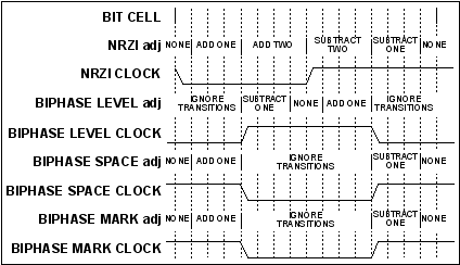
Figure 17-2 shows the adjustment ranges and output clock for the different modes of operation of the DPLL. Each mode of operation will be described in turn.
- In the biphase-level mode this means the transition that defines the last zero of the closing flag.
- In the biphase-mark and the biphase-space modes this means the transition that defines the end of the last zero of the closing flag.
With NRZ and NRZI encoding, all transitions occur on bit-cell boundaries and the data should be sampled in the middle of the bit cell. If a transition occurs after the expected bit-cell boundary (but before the midpoint), the DPLL needs to lengthen the count to line up the bit-cell boundaries. This corresponds to the "add one" and "add two" regions shown. If a transition occurs before the bit-cell boundary (but after the midpoint), the DPLL needs to shorten the count to line up the bit-cell boundaries. This corresponds to the "subtract one" and "subtract two" regions shown. The DPLL makes no adjustment if the bit-cell boundaries are lined up within one count of the divide-by-16 counter. The regions that adjust the count by two allow the DPLL to synchronize faster to the data stream when starting up.
With biphase-level encoding, there is a guaranteed "clock" transition at the center of every bit cell and optional "data" transitions occur at the bit cell boundaries. The DPLL only uses the clock transitions to track the bit-cell boundaries by ignoring all transitions occurring outside a window around the center of the bit cell. This window is half a bit cell wide. Additionally, because the clock transitions are guaranteed, the DPLL requires that they always be present. If no transition is found in the window around the center of the bit cell for two successive bit cells, the DPLL is not in lock and immediately enters the search mode. The search mode assumes that the next transition seen is a clock transition and immediately synchronizes to this transition. No clock output is provided to the receiver during the search operation. Decoding biphase-level data requires that the data be sampled at either the quarter or three-quarter point in the bit cell. The DPLL here uses the quarter point to sample the data.
Biphase-mark encoding and biphase-space encoding are identical as far as the DPLL is concerned, and are similar to biphase-level encoding. The primary difference is the placement of the clock and data transitions. With these encodings the clock transitions are at the bit-cell boundary, the data transitions are at the center of the bit cell, and the DPLL operation is adjusted accordingly. Decoding biphase-mark or biphase-space encoding requires that the data be sampled by both edges of the recovered receive clock.
17.4 Register Descriptions
Returns the contents of the receive buffer.
Loads the transmit buffer with a data byte for transmission.
Returns the contents of the receive buffer.
Loads the transmit buffer with an address byte, marked with a "one" address bit, for transmission.
Eight LSBs of the divider that generates the serial clock for this channel. This divider is not used unless the MSB of the corresponding SxDHR is set to one.
| Rabbit Semiconductor www.rabbit.com |