User's Manual
|
|
| Rabbit 4000 Microprocessor User's Manual |
|
16. Serial Ports A – D
16.1 Overview
Serial Ports A, B, C, and D are identical, except for the source of the data clock and the transmit, receive, and clock pins. Serial Port A is special because it can be used to bootstrap the processor. Each serial port can be used in the asynchronous or the clocked serial mode with an internal or external clock.
In the asynchronous mode, either 7 or 8 data bits can be transferred, and a parity bit and/or an additional address (0) or long stop (1) bit can be appended as well. Parity and the address/long stop bits are also detected when they are received. The asynchronous mode is full-duplex, while the clocked mode can be half or full-duplex.
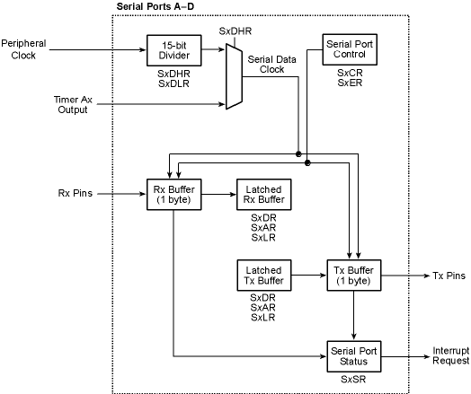
Both transmit and receive have one byte of buffering — a byte may be read while another byte is being received, or the next byte to be transmitted can be loaded while the current byte is still being transferred out. The byte is available in the buffer after the final bit is sampled.
The status of each serial port is available in the Serial Port Status Registers (SxSR), and contains information on whether a received byte is available, the receive buffer was overrun, a parity error was received, and the transmit buffer is empty or busy sending a byte. The status is updated when the final bit of a received byte is sampled, or when the final bit of a transmitted byte is sent out. Each serial port has a separate interrupt vector that will be requested whenever the transmit buffer is emptied or the receive buffer contains a full byte.
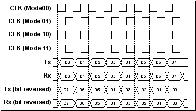
All four common SPI clock modes are supported, and the bit order of the data may be either MSB or LSB first. The transmit and receive operations are under program control as well.
In the asynchronous mode, IrDA-compliant RZI encoding can be enabled to reduce the bit widths to 3/16 the normal width (1/8 the normal width if the serial data clock is 8× instead of 16× ), which allows the serial port signal to be connected directly to an IrDA transceiver.
It is possible to select the same pin on Parallel Port C for both transmit and receive operation. This allows glueless support for bidirectional serial protocols.
It is possible to synchronize a clocked serial transfer to the match registers of Timer B to generate precisely timed transmissions.
The serial port data clocks can be generated from the appropriate 8-bit timer from Timer A shown in Table 16-1 or from a dedicated n+1 15-bit divider. In either case, the resulting byte data rate in the asynchronous mode is 1/8 or 1/16 the data clock rate (selectable). However, in the clocked serial mode the byte data rate is equal to the data clock rate as generated from the appropriate Timer A timer or from the dedicated 15-bit divider.
When Serial Port A is used in the asynchronous bootstrap mode, the 32 kHz clock is used to generate the expected 2400 bps data rate. An external clock must be supplied for the clocked serial bootstrap mode.
The behavior of the serial port during a break (line held low) is configurable; character assembly can continue during the break condition to allow for timing the break, or character assembly can be inhibited to reduce the interrupt overhead.
16.1.1 Block Diagram
16.1.2 Registers
16.2 Dependencies
16.2.1 I/O Pins
Serial Port A can transmit on parallel port pins PC7, PC6, or PD6, and can receive on pins PC7, PD7, or PE7. If the clocked serial mode is enabled, the serial clock is either transmitted or received on PB1. When an internal clock is selected in the clocked serial mode, PB1 is automatically enabled as a clock output.
Serial Port B can transmit on parallel port pins PC5, PC4, or PD4, and can receive on pins PC5, PD5, or PE5. If the clocked serial mode is enabled, the serial clock is either transmitted or received on PB0. When an internal clock is selected in the clocked serial mode, PB0 is automatically enabled as a clock output.
Serial Port C can transmit on parallel port pins PC3 or PC2, and can receive on pins PC3, PD3, or PE3. If the clocked serial mode is enabled and 8-bit memories are used, the serial clock will be transmitted on PD2, and can be received on either PD2 or PE2. The serial clock may also be transmitted on PC7, PD7, or PE7. When 16-bit memories are used, the serial clock can be transmitted on PC7 or PE7, and can be received on PD2 or PE2.
NOTE When Serial Port C is used as a clocked serial port and 8-bit memories are used, the serial clock is transmitted on PD2, and so PD2 will not be available for other use. Serial Port D can transmit on parallel port pins PC1 or PC0, and can receive on pins PC1, PD1, or PE1. If the clocked serial mode is enabled and 8-bit memories are used, the serial clock will be transmitted on PD0, and can be received on either PD0 or PE0. The serial clock may also be transmitted on PC3, PD3, or PE3. When 16-bit memories are used, the serial clock can be transmitted on PC3 or PE3, and can be received on PD0 or PE0.
NOTE When Serial Port D is used as a clocked serial port and 8-bit memories are used, the serial clock is transmitted on PD0, and so PD0 will not be available for other use.
Table 16-2. Pin Usage Serial Ports A – D
16.2.2 Clocks
The data clocks for Serial Ports A – D are based on the peripheral clock and are divided by either a Timer A divider or a dedicated 15-bit divider. In either case, the overall clock divider will be the value in the appropriate register plus one.
16.2.3 Other Registers
16.2.4 Interrupts
A serial port interrupt can be generated whenever a byte is available in the receive buffer or when a byte is finished being transmitted out of the transmit buffer.
The serial port interrupt vectors are located in the IIR as follows.
- Serial Port A at offset 0x0C0
- Serial Port B at offset 0x0D0
- Serial Port C at offset 0x0E0
- Serial Port D at offset 0x0F0
Each of them can be set as Priority 1, 2, or 3 in SxCR, where x is A – D for the four serial ports.
16.3 Operation
16.3.1 Asynchronous Mode
The following steps explain how to set up Serial Ports A – D for asynchronous operation. The serial ports can be used by polling the status byte, but their performance will be better with an interrupt. These instructions also apply to the asynchronous operation of Serial Ports E – F.
- Write the interrupt vector for the interrupt service routine to the internal interrupt table.
- Set up the desired transmit pin by writing to the appropriate parallel port function register (PxFR) and alternate output register (PxALR or PxAHR).
- Select the appropriate mode by writing to SxCR (receive input port and 7 or 8 bits). Also select the interrupt priority.
- Select additional options by writing to SxER (parity, RZI encoding, clock polarity, and behavior during break).
- Write the desired divider value to TATxR for the appropriate serial port, or else write a divider value to the dedicated 15-bit divider in SxDLR and SxDHR. If the dedicated divider is to be used, write a 1 to the most-significant bit of SxDHR to enable it.
A sample asynchronous serial interrupt handler is shown below for Serial Port A.
async_sera_isr::
   push af             ; save used registers
   ioi ld a, (SASR)    ; get status
   bit a,7               ; check if byte ready in RX buffer
   push af             ; save status for next check
   jr  z, check_for_tx
rx_ready:
   ioi ld a, (SADR)    ; read byte and clear interrupt

   ; do something with byte here

check_for_tx:
   pop af
   bit a,3               ; check if TX buffer was emptied
   jr nz, done

   ; get next byte to be transmitted into A here

   ioi ld (SADR), a    ; load next byte into TX buffer and clear interrupt
done:
   pop af              ; restore used registers
   ipres
   ret
To transmit with an address (1) bit appended, write the data to SxAR instead of SxDR; to append a long stop (0) bit write to SxLR instead.
16.3.2 Clocked Serial Mode
The following steps explain how to set up Serial Ports A – D for the clocked serial mode. When the internal clock is selected, the Rabbit 4000 is in control of all transmit and receive operations. When an external clock is selected the other device controls all transmit and receive operation. For both situations the decision between polling and interrupt-driven methods is application dependent.
write the byte to SxDR and then write 10 (or 11) to bits 6-7 of SxCR to enable the transfer;
- Write the interrupt vector for the interrupt service routine to the internal interrupt table.
- Set up the desired data transmit and clock pins by writing to the appropriate parallel port function register (PxFR) and alternate output register (PxALR or PxAHR).
- Select the appropriate mode by writing to SxCR (receive input port and clock source). Also select the interrupt priority.
- Select additional options by writing to SxER (clock polarity, bit order, and clock source if external).
- Write the desired divider value to TATxR for the appropriate serial port, or else write a divider to the dedicated 15-bit divider in SxDLR and SxDHR. If the dedicated divider is to be used, write a 1 to the most-significant bit of SxDHR to enable it.
- There are two methods to transfer a byte:
write the byte to SxAR which will automatically start the transfer.
- To receive a byte, write 01 to bits 6-7 of SxCR to start the receive operation. If the internal clock is selected, the clock will begin immediately and the data will be read; if an external clock is selected, the receive will occur when the clock is detected.
A sample clocked serial interrupt handler is shown below for Serial Port B.
clocked_serb_isr::
   push af             ; save used registers
   ioi ld a, (SASR)    ; get status
   bit a,7               ; check if byte ready in RX buffer
   push af             ; save status for next check
   jr  z, check_for_tx
rx_ready:
   ioi ld a, (SADR)    ; read byte and clear interrupt

   ; do something with received byte here

   ld a, 0x41          ; set bits 6-7 to 01, the other bits should
                       ; represent the desired SACR setup

   ioi ld (SACR), a    ; start a new receive operation

check_for_tx:
   pop af
   bit a,3               ; check if TX buffer was emptied
   jr nz, done

   ; get next byte to be transmitted into A here

   ioi ld (SADR), a    ; load TX buffer with next byte and clear interrupt
done:
   pop af              ; restore used registers
   ipres
   ret
16.4 Register Descriptions
Returns the contents of the receive buffer.
Loads the transmit buffer with a data byte for transmission.
Returns the contents of the receive buffer.
Loads the transmit buffer with an address byte, marked with a "one" address bit, for transmission.
Eight LSBs of the divider that generates the serial clock for this channel. This divider is not used unless the MSB of the corresponding SxDHR is set to one.
| Rabbit Semiconductor www.rabbit.com |