
User's Manual
|
|
| Rabbit 2000 Microprocessor User's Manual |
|
Appendix B. Rabbit 2000 Revisions
B.1 Rabbit 2000 Revisions
Since its release, the Rabbit 2000 microprocessor has gone through a number of revisions. The revisions reflect bug fixes, improvements, and the introduction of new features. All Rabbit 2000 revisions are pin-compatible and transparently replace previous versions of the chip.
The Rabbit 2000 has been supplied in the following versions.
(a) Certain instructions did not function correctly as described in Technical Note TN302, Rabbit 2000 Instruction Bug. The Dynamic C compiler corrects this situation automatically.
- Original Rabbit 2000--identified by IQ2T on the package. This original Rabbit 2000 began shipping in November,1999, and was phased out in January, 2002. There were several bugs:
(b) The external interrupt inputs had to be tied together with a resistor as described in Technical Note TN301, Rabbit 2000 Microprocessor Interrupt Problem.
(c) Wait states did not function properly when used to access code in slower memories because certain instructions failed in these circumstances. This bug is fixed in the Rabbit 2000A through Rabbit 2000C revisions.
(a) Support for separate I & D space.
- First revision (Rabbit 2000A)--identified by IQ3T on the package. This version began shipping in January, 2002. All the bugs in the original Rabbit 2000 were fixed, and additional new features were added:
(b) An additional register in the serial port hardware simplifies sending out an additional stop bit or parity bit.
(c) Improvements in the battery-backup hardware allow for implementation of a simplified circuit for backing up the real-time clock and associated static RAM. A new bug exists in the block copy instruction between separate I & D spaces that is only active when the separate I & D space is enabled. This bug is automatically corrected by Dynamic C.
- Second revision (Rabbit 2000B)--identified by IQ4T on the package. This version began shipping in samples and very low volume to select customers having problems with EMI in April, 2002. This part was phased out and will be replaced by the Rabbit 2000C for volume orders. This version has the clock spectrum spreader, but lacks the early I/O enable, which results in tight specifications for memory I/O enable. The clock doubler unit uses codes incompatible with earlier revisions. Furthermore, a problem with LDIR/LDDR operation and Instruction/Data split was discovered. These problems are all corrected in the Rabbit 2000C.
- Third revision (Rabbit 2000C)--identified by IQ5T on the package. Z-World and Rabbit Semiconductor products using the Rabbit 2000 chip will begin using the Rabbit 2000C chip in November, 2002. This version is the same as the Rabbit 2000B, except that the early I/O enable is implemented and the clock doubler codes are compatible with earlier versions. Although the LDIR/LDDR bug outlined in the Rabbit 2000B description is fixed, a new bug related to block move operations and wait states was discovered. This bug is automatically corrected by Dynamic C.
Rabbit 2000 chips identified by UQ5T on the package are RoHS-compliant. The UQ5T RoHS versions were introduced in 2007, and both IQ5T and UQ5T versions are presently avaialble.
B.2 Discussion of Fixes and Improvements
Table B-1 lists bug fixes, improvements, and additions for the various revisions of the Rabbit 2000.
Table B-1. Summary of Rabbit 2000 Fixes and Improvements Description Rabbit 2000 (IQ2T) Rabbit 2000A (IQ3T) Rabbit 2000B (IQ4T) Rabbit 2000C (IQ5T/
UQ5T1)ID Registers for version/revision identification.
Added Long Stop Register for asynch 9-bit operation.
Added clocked serial command for full-duplex operation.
Improved battery-backup hardware.
Added support for Instruction/Data split.
Implemented write inhibit (/WE0) after reset.
Chip selects inactive during internal I/O.
Corrected external interrupt input bug.
Corrected IOI/IOE prefix bug.
Corrected DDCB/FDCB instruction bug.
Corrected wait-state bug.
Corrected LDIR/LDDR Instruction/Data split bug.
Added clock spectrum spreader module.
Added early I/O enable feature.
1 RoHS version
B.2.1 Rabbit Internal I/O Registers
Table B-2 summarizes the reset state of the new I/O registers added in the Rabbit 2000 revisions.
B.2.2 Revision-Level ID Register
Two read-only registers are provided to allow software to identify the Rabbit microprocessor and recognize the features and capabilities of the chip. Five bits in each of these registers are unique to each version of the chip. One register identifies the CPU (GCPU), and the other register is reserved for revision identification (GREV). The CPU identification (GCPU) of all revisions of the Rabbit 2000 microprocessor is the same. Rabbit 2000 revisions are differentiated by the value in the GREV register.
Table B-3 summarizes the processor identification information for the different Rabbit 2000 versions.
Table B-3. Rabbit 2000 Revision Identification Information Processor Revision Package Identifier GCPU [4:0] GREV [4:0] Rabbit 2000
Rabbit 2000A
Rabbit 2000B
Rabbit 2000C
Details of the CPU ID registers are listed in Table B-4 and Table B-5.
B.2.3 Serial Port Changes
Two features were added to the Rabbit 2000 serial port hardware in revisions A-C to improve and simplify asynchronous serial and clocked serial communication.
In the asynchronous transmission mode, serial data are transmitted in the following order.
Table B-6. Asycnchronous Serial Data Transmission Order Start Data Bits Stop Bit or Special Flag Stop Bit
In the original Rabbit 2000 it was difficult to transmit the additional stop bit. This could only be done by inserting a time delay before the next byte was transmitted. An additional register, the long stop register, was added in revisions A-C. The register serves as an alternate data-out register, and data stored in this register will be transmitted with 2 stop bits (high level at the Tx pin). This simplifies implementing "9th bit" protocols as well as sending parity for compatibility with legacy systems. With the new register, data may be conveniently transmitted with either a "1" or "0" bit inserted following the last data bit, and that bit will then be followed by a stop bit.
Section 12.6 and Section 12.7 provide additional information about asynchronous serial data transmission.
The Serial Port x Long Stop Register (SxLR) is only present in revisions A-C.
To initiate basic sending or receiving in the clocked serial mode, a command must be issued by writing to bits (7,6) of the control register for each byte sent or received. There is one command is to send a byte, and a different command to receive a byte. For full-duplex communication, it is necessary that a Tx command be issued first, followed within one-half bit time by the Rx command. The new feature added to revisions A-C contains a command that initiates a transmit and receive at the same time for better support of full-duplex communication.
B.2.4 Improved Battery-Backup Circuit
Improvements were made in revisions A-C to reduce the internal power consumption of the RTC circuit. In addition, external circuitry was designed to further reduce power consumption by the overall oscillator circuit in board-level products based on the Rabbit 2000.
An external low-current oscillator can be built using an inexpensive single-gate (tiny logic) unbuffered inverter. The current consumption of this circuit is about 4 µA with a 2 V supply. Using this circuit, oscillation continues even when the voltage drops to 0.8 V, and oscillation is still very strong at 1.2 V. The oscillator should have its exposed circuit traces conformally coated to prevent the possibility of loading the circuit by conduction on the PC board surface in a moist atmosphere. (Rabbit Semiconductor has published an application note on conformal coating, Technical Note TN303, Conformal Coatings.)
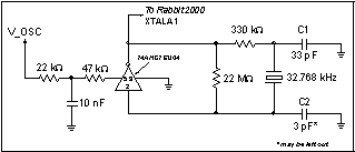
The capacitors on either side of the crystal provide the load capacitance, which is specified by the crystal manufacturer. Typically the load capacitance is about 12 pF. This is the capacitance that should be in parallel with the crystal for it to operate at the specified frequency. C1 and C2 provide this load capacitance. The formula for the load capacitance is
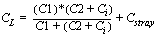
This is just the formula the capacitance of two capacitors in series plus any stray capacitance in the board layout, perhaps 2 pF. Note that the input capacitance of the gate (Cin) must also be taken into account. The gate input capacitance is not constant, but is a function of frequency. Thus if it is measured, it should be done with a sine-wave generator operating at 32 kHz. The output capacitance is not relevant because the 330 kW resistor isolates it from the crystal. If C2 is made smaller, this will increase the voltage swing on the gate input and allow the oscillator to operate at a lower voltage. This oscillator will start at about 1.2 V and operate down to about 0.75 V. The 47 kW resistor limits the short-circuit current when the CMOS gate is switching, and thus limits the overall current consumption. The 330 kW resistor is needed to limit crystal drive at higher operating voltages, but if the 330 kW resistor is too large, it will adversely affect low-voltage operation.
Typical 32.768 kHz crystals are specified for a maximum drive level of 1 µW. A modest overdrive, perhaps 100% over this limit, will most likely have not any adverse effects except to cause the crystal to age more rapidly than specified. Aging is a gradual change of frequency of about 3 parts per million, and is most significant in the first few months of operation. The drive power can be computed from P = (I2) * R, where I is the RMS AC current and R is the effective resistance of the crystal. Typical values for R are 20 kW for 32.768 kHz turning-fork crystals. Maximum values are often specified as 35 kW or 50 kW. If the effective resistance is 20 kW, then 1 µW of power is reached when I = 7 µA (RMS). It is logical to use the typical effective resistance rather than the maximum total resistance in computing drive power. If a particular crystal has a higher resistance, this indicates that it is losing more energy on each oscillation, perhaps because of surface contamination, and thus requires more power to sustain the same amplitude of physical flexure of the quartz. Thus the stress on the quartz will not be greater even though the drive power is greater for a unit that happens to have an effective resistance of 35 kW rather than the typical value of 20 kW. The current can be measured directly with a sensitive current probe, but it is easier to calculate the current by measuring the voltage swing at the gate input with a low-capacitance oscilloscope probe. The RMS voltage at this point is related to the RMS current by the relationship
- I = Vrms * w * Ctotal
- Ctotal = C2 + Ci + Cprobe
- w = 2p * 32768
- Vrms = 0.707 * Vp-p
If Ctotal = 12 pF, and the effective resistance is 20 kW, then the current (in µA) and the drive power (in µW) are given by
- I = 2.5 * Vrms
- P = 0.125 * (Vrms)2
- I = 1.75 * Vp-p
- P = 0.061 * (Vp-p)2
For a 5 V p-p swing, the power is 1.5 µW. The power is 1.0 µW for 4 V p-p, and the power is 0.5 µW for 3 V p-p.
TN235, External 32.768 kHz Oscillator Circuits, provides further information on oscillator circuits and crystals.
B.2.5 Added Support for Instruction/Data Split
This option is available on revisions A-C. Code generated for the Rabbit 2000A will run on the Rabbit 2000B or 2000C, but not vice versa. The separate I & D space allows the root segment and the data segment, normally the first 52K of the 64K address space, to be mapped into separate spaces for instruction fetch (I space) and data fetch or store (D space). The advantage of this is that the size of the root data space can be expanded up to 52K without interfering with the root code space. The root code space, which has certain special properties, particularly faster subroutine linkage, can be expanded to fill up to 52K of root space. Formerly both spaces had to share the 52K of space. Separate I & D space is supported by Dynamic C version 7.30 or later. The data space is normally split into separate parts, one part for constants mapped to flash memory and the other part for variables mapped to RAM. The code space is mapped into the first 52K of flash memory. This option expands the size of root data and code while preserving the advantages of using the root, which may be accessed by 16-bit addresses. Use of the option is generally transparent for Dynamic C users. More information on separate I & D implementation will be available in the Rabbit 2000 Designer's Handbook, and is currently available in the Rabbit 3000 Designers Handbook.
The MMIDR register shown in Table B-9 is used to enable and configure separate I & D space support in addition to the /CS1 enable option used to improve the access time of battery-backable SRAM.
NOTE Bits [7:5] and [3:0] were always written with zero in the original Rabbit 2000 chip.
B.2.6 Write Inhibit (/WE0) After Reset
This feature, available in revisions A-C, modified the reset state of the MB0CR register to inhibit /WE0. Inhibiting writes after reset prevents the processor from inadvertently writing to an unprogrammed flash memory that doesn't have the software data protection enabled. In a flash memory where the software data protection is enabled, an inadvertent write will temporarily disable the flash memory if the memory is used to execute code.
This has not been a serious problem in the past for two reasons. First, programming systems using Dynamic C permanently enable software data protection, and second, most manufacturers ship their memory devices with software data protection permanently enabled.
Software data protection consists of a three-byte load sequence that is used to initiate program operation during the system power-up or power-down, providing protection from inadvertent write operations. Flash devices usually provide a chip-erase operation, which allows the user to erase the entire memory array to the `1's state. Flash devices are normally erased prior to shipment. When the Rabbit processor comes out of reset, it begins fetching instructions from address zero of the device connected to /CS0, /OE0, and /WE0, which in most cases is a flash memory. If the flash contains 0xff at address zero, the processor will decode this as an RST 38. An RST 38 vectors to an ISR area at address 0x70 and pushes the PC onto the stack, which by default is located at address 0x00 (flash memory). This can be a problem if the flash is repeatedly written to in an endless loop because flash memories can only endure a finite number of writes, typically about 100,000.
B.2.7 Chip Selects Inactive During Internal I/O
In the original Rabbit 2000, it was found that whichever chip select was mapped to MB0CR would become active during internal I/O operations. This behavior did not cause any problems, but was corrected in revisions A-C.
B.2.8 External Interrupt Input Bug Fix
The external interrupt bug discovered in the original Rabbit 2000 required the external interrupt inputs to be tied together with a resistor as described in Technical Note TN301, Rabbit 2000 Microprocessor Interrupt Problem. This bug was subsequently fixed in revisions A-C of the Rabbit 2000, and two separate external interrupt inputs are available on these devices.
B.2.9 IOI/IOE Prefix Bug Fix
Certain instructions did not function correctly as described in Technical Note TN302, Rabbit 2000 Instruction Bug. The problem was corrected in revisions A-C of the Rabbit 2000.
B.2.10 DDCB/FDCB Instruction Page and Wait State Bug Fixes
Four-byte instructions starting with DD-CB or FD-CB didn't work when attempted with wait states.
The fetch of the byte immediately following the instruction did not have the correct number of wait states inserted for the following instructions only when using wait states. Rather than the programmed number of wait states, the fetch was short by one wait state.
DJNZ (branch not taken only)
JR cc (branch not taken only)
JP cc (branch not taken only)
A similar thing happens for the block move instructions. In these cases, the read cycle is short by one wait state.
LDDR
LDIR
For the multiply instruction, the fetch of the first byte after the MUL instruction had no wait states, independent of the number programmed.
These problems were corrected in revisions A-C of the Rabbit 2000.
A new LDIR/LDDR bug was discovered in September, 2002. The problem has to do with wait states and the block move operations. With this problem, the first iteration of
LDIR/LDDRuses the correct number of wait states for both the read and the write. However, all subsequent iterations use the number of waits programmed for the memory located at the write address for both the read and write cycles. This becomes a problem when moving a block of data from a slow memory device requiring wait states to a fast memory device requiring no wait states. With respect to external I/O operations, theLDIRorLDDRperforms reads with zero wait states independent of the waits programmed for the I/O for all but the first iteration. The first iteration is correct. This bug is automatically corrected by Dynamic C.B.2.11 LDIR/LDDR Instruction/Data Split Bug Fix
The bug with
LDIR/LDDRand separate I & D space discovered in the Rabbit 2000A had to do with the way the memory control unit treated the move from and the move to addresses of the block move operation. With the instruction/data split enabled, data access in the ROOT and/or DATASEG regions would result in addresses A16 and/or A19 being inverted, depending on how the MMIDR was configured. This would allow the data space to be moved up or down by 64K or 512 K.With this problem, the first iteration of
LDIR/LDDRresulted in the correct address inversion for data accesses in the ROOT and/or DATASEG regions. However, all subsequent iterations took place in the code region (without any address inversion).This problem was fixed in revisions B and C of the Rabbit 2000.
B.2.12 Clock Spectrum Spreader Module
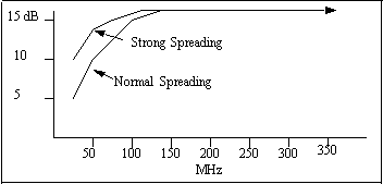
This is a feature introduced on the Rabbit 3000 and migrated to revisions B and C of the Rabbit 2000. The clock spectrum spreader and early memory output enable are turned on by default for the Rabbit 2000C in Dynamic C version 7.32 and higher. The spectrum spreader is very powerful for reducing EMI because it will reduce all sources of EMI above 100 MHz that are related to the clock by about 15 dB. This is a very large reduction since it is common to struggle to reduce EMI by 5 dB in order to pass government tests.
The spectrum spreader modulates the clock so as to spread out the spectrum of the clock and its harmonics. Since the government tests use a 120 kHz bandwidth to measure EMI, spreading the energy of a given harmonic over a wider bandwidth will decrease the amount of EMI measured for a given harmonic. The spectrum spreader not only reduces the EMI measured in government tests, but it will also often reduce the interference created for radio and television reception.
The spectrum spreader has three settings under software control: off, normal spreading, and strong spreading.
Two registers control the clock spectrum spreader. These registers must be loaded in a specific manner with proper time delays. GCM0R is only read by the spectrum spreader at the moment when the spectrum spreader is enabled by storing 0x080 in GCM1R. If GCM1R is cleared (when disabling the spectrum spreader), there is up to a 500-clock delay before the spectrum spreader is actually disabled. The proper procedure is to clear GCM1R, wait for 500 clocks, set GCM0R, and then enable the spreader by storing 0x080 in GCM1R.
When the spectrum spreader is engaged, the frequency is modulated, and individual clock cycles may be shortened or lengthened by an amount that depends on whether the clock doubler is engaged and whether the spectrum spreader is set to the normal or strong setting. The frequency modulation amplitude and the change in clock cycle length is greater at lower voltages or higher temperatures since it is sensitive to process parameters. The spectrum spreader also introduces a time offset in the system clock edge and an equal offset in edges generated relative to the system clock. A feedback system limits the worst-case time error of any signal edge derived from the system clock to ±35 ns for the normal setting and ±70 ns for the strong setting at 5.0 V. The maximum time offset is inversely proportional to operating voltage. This small timing error will not generally affect operations in the great majority of systems.
If the input oscillator frequency is 4 MHz or less, the spectrum spreader modulation of frequency will enter the audio range of 20 kHz or less, and may generate an audible whistle in FM stations. For this reason it may be desirable to disable the spreader for low-speed oscillators (where it is probably unnecessary anyway). However, in practical cases the whistle may not be audible because of the very low level of the interference from a system with a low oscillator frequency with the spectrum spreader engaged. Each halving of clock frequency reduces the amplitude of the harmonics at a given frequency by 6 dB or more.
The effect of pure harmonic noise on an FM station is to either completely block out a station near the harmonic frequency or to disturb the reception of that station. If the spectrum spreader is engaged, the interference will be spread across the band, but will generally be so low as to be undetectable, except perhaps for extremely weak stations. The effect of a pure harmonic on TV reception is to create a herringbone pattern created by a harmonic falling within the station's band. If the spreader is engaged, the pattern will disappear unless the station is very weak, in which case the interference will be seen as noise distributed over the screen.
A more important change in timing is that the memory access time will be shortened. The shortening with the clock doubler enabled and zero wait states is a maximum of 6 ns in the normal mode and 9 ns in the strong mode. Only one of the 2 clocks in a memory cycle will be shortened.
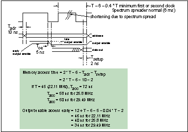
If the clock doubler is not enabled, then the maximum shortening will be 9 ns in the normal mode and 18 ns in the strong mode. Figure B-3 assumes that the combined address out and data setup in is 12 ns. The time from clock to output enable is assumed to be 5 ns. The maximum asymmetry of the clock is assumed to be 52-48%, which shortens one clock by 4% and lengthens the other by 4% if the clock is doubled.
Early output enable is enabled by default on the Rabbit 2000C, but may be disabled. The clock low time is controlled by the clock doubler control register, and is assumed to be a minimum of 14 ns in the above example. Also the maximum clock speed from the example with the spreader enabled and 55 ns memory with 25 ns output enable is 25.8 MHz. At 29.49 MHz the memory access must be 50 ns, and the spectrum spreader must be turned off, or a wait state must be added. Operation with a doubled clock and the spreader enabled at 29.49 MHz is only allowed for T < 70°C and V > 4.75 V since the instantaneous clock frequency bursts to 38.5 MHz when the spectrum spreader and clock asymmetry together produce maximum shortening of a clock cycle.
B.2.13 Early Memory Output-Enable Feature
The early I/O enable feature was added to the Rabbit 2000C revision to relax the tight timing requirements for memory access when using the clock spectrum spreader. The early I/O option extends the output enable time for the /OEx strobes and the write enable time for the /WEx strobes by a half clock cycle. The Memory Timing Control Register (MTCR) enables the extended timing for the memory output enable and write enable strobes.
Memory read and write timing are discussed further in Chapter 15, "AC Timing Specifications."
| Rabbit Semiconductor www.rabbit.com |