
User's Manual
|
|
| Rabbit 2000 Microprocessor User's Manual |
|
15. AC Timing Specifications
The Rabbit 2000 processor may be operated at voltages between 2.5 V and 5.5 V, and at temperatures from -40°C to +85°C with use possible use over the range -55°C to +120°C. Most users will operate the Rabbit at either 5.0 V or 3.3 V. The most computation per watt is obtained at approximately 3.3 V. The highest practical speed is usually obtained at 5 V.
The Rabbit is available in one version, which has a maximum clock speed of 29.4 MHz over the industrial temperature range of -40°C to +85°C. The R30 has a maximum clock speed of 18.9 MHz at 3.3 V ±10%. The maximum clock speed is 11.5 MHz at 2.5 V.
If a half-speed crystal is used with the clock doubler to achieve the desired clock speed, the maximum clock speed must be reduced by 4% to allow for an up to 4% asymmetry (52/48) in the waveform generated by the oscillator. This is because the clock doubler uses the intermediate edge to generate the double frequency. If the clock doubler is used to double 14.7456 MHz to 29.4912 MHz, the operating temperature should be limited to 70°C.
To optimize power consumption, the usual strategy is to use a supply voltage between 3 V and 3.5 V, and the clock speed should be adjusted downward as far as feasible. This will give the maximum computation per watt.
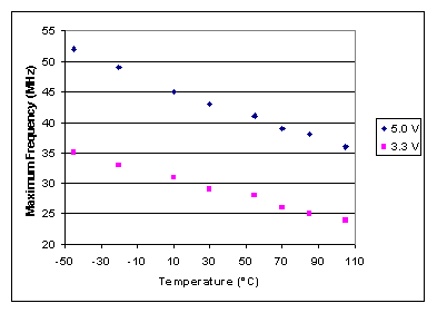
The industrial clock speed values in Table 15-1 (at a maximum temperature of 85°C) are improved by 7% over commercial ratings at 70°C (which are extended to -40°C here). The effect of temperature alone is a clock speed that is approximately 1.2% lower for each 5°C temperature increase. The maximum clock speed is approximately directly proportional to the operating voltage.
If serial communication is to be used at standard baud rates, then certain clock speeds must be used. These clock speeds are usually multiples of 1.8432 MHz to ensure that baud rates of 57,600 bps, 19,200 bps, and less will be available. Multiples of 3.6862 MHz ensure that baud rates of 115,200 bps, 38,400 bps, and less will be available. Multiples of 1.2288 MHz ensure that baud rates of 38,400 bps and less will be available. The standard Rabbit BIOS will accept any clock speed that is a multiple of 0.6144 MHz.
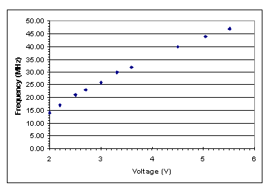
The graphs in Figure 15-1 and Figure 15-2 illustrate the maximum clock speed at which no failure is detected for a typical Rabbit 2000 as the voltage and temperature are varied. The official design specifications specify a lower maximum frequency to allow for process variation.
The die suffers significant self-heating at higher clock speeds. The die to ambient thermal impedance is 44°C/W at zero air flow. At 5 V and a current consumption of 65 mA, this would result in about 15°C of self-heating, and would reduce the maximum clock speed by approximately 3%. This reduction is included in Table 15-2, which provides the memory access time requirements.
When interfacing to memory devices, the memory access time required for a directly interfaced memory is given by:
where Tadr is the delay between the rising edge of T1 and address valid, and Tsetup is the data setup time relative to the clock. Tadr and Tsetup are shown in Figure 15-3 to Figure 15-4 for memory read/write and I/O read/write cycles. Most 5 V memories are TTL compatible in that they switch at 0.8 V and 2.0 V. Tsetup is specified from the point at which the input voltage reaches 30% or 70% of VDD for falling and rising signals respectively. Toe is specified for the time from the clock that is required for the signal to reach 0.8 V.
The Tadr measured was the time required for the signal to fall from a high level to 0.8 V. Tadr depends on the bus loading--address line A0 has a more powerful driver and can handle double the capacitance with the same delay times. The Tadr times also apply to the memory chip select lines.
The formula in Equation (1) remains true if the clock doubler is used, except that the access time must be reduced by 4% of one clock period if there is an odd number of wait states. The length of the Toe pulse is subjected to a reduction of up to 4% if the clock doubler is used.
15.1 Memory Access and I/O Read/Write Times
The memory access time requirements are listed in Table 15-2. It is important that wait states should not be used for any memory that holds code that is being executed. Memory wait states are only intended for use with data accesses. For code memory the clock should be matched to the memory requirements, or one of the clock dividers should be enabled to accommodate slow memory. As a rough guide, each data memory wait state in main RAM that is introduced will reduce the average compute performance by approximately 8%. The data memory read access is slowed by 50% for 1 wait state and is slowed by 100% for 2 wait states. However, since only a small proportion of accesses are data accesses rather than code accesses or instruction fetch cycles, the overall affect on performance is slight. If data memory wait states are introduced, it is important to use the macros specified in the BIOS so that the compiler will be aware of the wait states.
Generally, the maximum operating speed is proportional to the power supply voltage. The operating current is proportional to the voltage, and so the operating power is proportional to the square of the voltage. The operating power is also proportional to the clock speed. Higher temperatures reduce the maximum operating speed by approximately 1% for each 5°C. In addition, higher operating speeds increase the die temperature because of the heat generated and therefore slightly compound the adverse effects of higher temperature.
Figure 15-3, Figure 15-4, and Figure 15-5 illustrate the memory and I/O read and write cycles. The Rabbit operates at 2 clocks per bus cycle plus any wait states that might be specified.
The following memory read time delays were measured.
The measurements were taken at the 50% points under the following conditions.
The following memory write time delays were measured.
The measurements were taken at the 50% points under the same conditions that the memory read delays were measured.
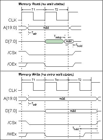
Notice that the data times are different, depending on whether data are being read or written. Thold for data read specifies how long the data must remain valid following the rising edge of T1 when the clock cycle repeats. TDHZV for data write specifies how long the data remain valid once /WEx goes high, and must be at least one-half of a CPU clock cycle.
The following I/O read time delays were measured.
The measurements were taken at the 50% points under the following conditions.
The following I/O write time delays were measured.
The measurements were taken at the 50% points under the same conditions that the I/O read delays were measured.
I/O bus cycles have an automatic wait state and thus require 3 clocks plus any extra wait states specified.
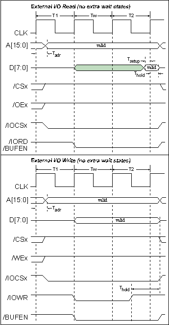
Figure 15-5 shows the effect of adding an extra wait state to the memory read/write cycles. The effects are similar for the I/O bus read/write cycles.
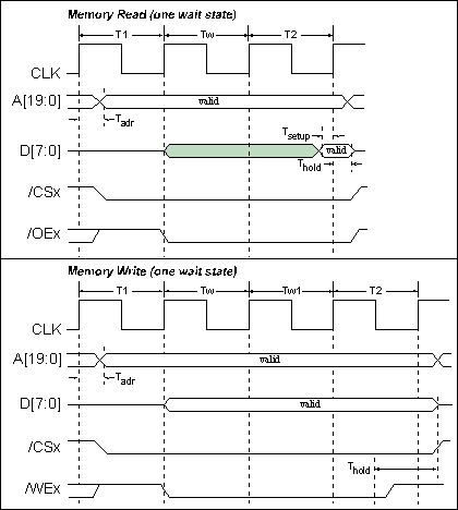
Table 15-7 provides typical memory and external I/O parameters measured at 3.3 V.
15.2 Current Consumption
Typical current is proportional to both clock frequency and voltage. The main oscillator requires approximately 6 mA at 5 V and 2 mA at 3 V independent of frequency. The basic current consumption for the processor exclusive of the oscillator at 5 V and 15 MHz is approximately 42 mA. The following formula can be used to compute the current consumption:
The first term represents the current consumed by the processor, which is directly proportional to voltage and frequency. The second term is the current consumed by the main oscillator, which is approximately independent of frequency, but varies as the square of the voltage. This term is zero when the main oscillator is disabled. Some checkpoints for current consumption are provided in Table 15-8.
The current consumed by memory and other devices included in the system, including pullup resistors, outputs driving a load, and floating inputs, must be added to the figures in Table 15-8.
The 32.768 kHz clock oscillator and the associated real-time clock consume approximately 23 µA at 3 V. (At 2.25 V, when backed by a battery, the current consumption is approximately 11 µA.) The (typical) current consumed when the main power is off, and only the 32.768 kHz oscillator and clock are powered, is given by the formula
where V is the operating voltage. This is the current that must be supplied by a backup battery, not counting the current required by the associated circuits. The oscillator will not operate below approximately 1.3 V. The measurement from which the above formula was derived were made with a series resistor of 390 kW and load capacitors of 15 pF in the 32.768 kHz oscillator circuit. The shunt resistor was 10 MW.
If the processor is running at 32.768 kHz, then the added current to operate the processor at room temperature (main oscillator shut off) is given by:
In low-power modes the current consumption is proportional to the square of the voltage. At 3.0 V this is approximately 67 µA. Add the 25 µA needed to operate the oscillator and the total current consumption will be approximately 92 µA with the processor operating at 32.768 kHz.
The current consumed by RAM or flash memory will be substantial and very significant at lower frequencies if auto powerdown flash or low-power RAM is not used. If low-power RAM is used to support the sleepy mode, the sleepy mode loop should be copied to RAM and executed in RAM. When trying to operate in an ultra low-power sleepy mode, it is important that no inputs be floating. Floating inputs consume substantial power. Keep in mind that port D open-drain outputs will create floating inputs if not pulled toward zero. Pullup resistors consume current and should be avoided or disabled in ultra low-power modes. When testing a sleepy mode of operation, it is advisable to connect an ammeter to make sure that no extra floating inputs or other current-consuming features are included in the setup.
| Rabbit Semiconductor www.rabbit.com |