
User's Manual
|
|
| Rabbit 2000 Microprocessor User's Manual |
|
10. I/O Bank Control Registers
The pins of Port E can be set individually to be I/O strobes. Each of the eight possible I/O strobes has a control register that controls the nature of the strobe and the number of wait states that will be inserted in the I/O bus cycle. Writes can also be suppressed for any of the strobes. The types of strobes are shown in Figure 10-1. Each of the eight I/O strobes is active for addresses occupying 1/8th of the 64K external I/O address space.
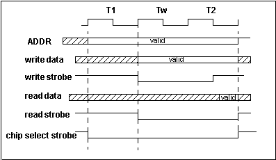
Table 10-1 shows how the eight I/O bank control registers are organized.
Table 10-1. I/O Bank Control Reg (adr IBxCR = 08xh) Bits 7,61 Bits 5,4 Bit 3 Bits 2-0 Wait state code
11-1
10-3
01-7
00-15
/IX strobe type
00--chip select
01--read strobe
10--write strobe
11--or of read and write strobe
1--permit write
0--inhibit write
Ignored
1 Total number of external I/O read/write wait states, including the one wait state that is always present.
Compared to memory read/write cycles, which are each 2 or 3 clock cycles long respectively, external I/O read/write cycles are always at least three clock cycles long.
The eight I/O bank control registers determine the number of I/O wait states applied to an external I/O access within the zone controlled by each register even if the associated strobes are not enabled.
The control over the generation of wait states is independent of whether or not the associated strobe in Port E is enabled. The upper 2 bits of each register determine the number of wait states. The four choices are 1, 3, 7, or 15 wait states. On reset, the bits are cleared, resulting in 15 wait states. The inhibit write function applies to both the Port E write strobes and the /IOWR signal.
These control bits have no effect on the internal I/O space, which does not have wait states associated with read or write access. Internal I/O read or write cycles are two clocks long.
The I/O strobes greatly simplify the interfacing of external devices. On reset, the upper 5 bits of each register are cleared. Parallel port E will not output these signals unless the data-direction register bits are set for the desired output positions. In addition, the Port E function register must be set to "1" for each position.
Each I/O bank is selected by the three most significant bits of the 16-bit I/O address. Table 10-2 shows the relationship between the I/O control register and its corresponding space in the 64K address space.
NOTE Refer to Section 3.3.8 for a fix to a bug that manifests itself if an I/O instruction (prefix IOI or IOE) is followed by one of 12 single-byte op codes that use HL as an index register.
| Rabbit Semiconductor www.rabbit.com |