
User's Manual
|
|
| Rabbit 2000 Microprocessor User's Manual |
|
11. Timers
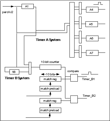
There are two timers--Timer A and Timer B. Timer A is intended mainly for generating the baud clock for the serial ports, a periodic clock for clocking parallel ports D and E, or for generating periodic interrupts. Timer B can be used for the same functions, but it cannot generate the baud clock. Timer B is more flexible when it can be used because the program can read the time from a continuously running counter and events can be programmed to occur at a specified future time.
Figure 11-1 shows a block diagram of Timers A and B.
11.1 Timer A
Timer A consists of five separate countdown timers--A1 and A4-A7--as shown in Figure 11-1.
Timers A1 and A4-A7 are 8-bit countdown registers as shown in Figure 11-2. The reload register can contain any number in the range from 0 to 255. The counter divides by (n+1). For example, if the reload register contains 127, then 128 pulses enter on the left before a pulse exits on the right. If the reload register contains zero, then each pulse on the left results in a pulse on the right, that is, there is division by one.
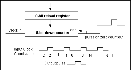
The timer systems are driven by the peripheral clock divided by two. This clock is always the same as the processor clock, or it is faster than the processor clock by a factor of eight. The output pulses are always one clock long. Clocking of the counters takes place on the negative edge of this pulse. When the counter reaches zero, the reload register is loaded on the next input pulse instead of a count being performed. The reload registers may be reloaded at any time since the peripheral clock is synchronous with the processor clock.
Timers A4, A5, A6 and A7 always provide the baud clock for serial ports A, B, C and D respectively. Except for very low baud rates, clock A1 does not need to be used to prescale the input clock for timers A4-A7. For example, if the system clock is 11.0592 MHz, and if the timer A4 divides by 144, an asynchronous baud rate of 2400 bps can be achieved in one step. The clock input to the serial port must be 16 times the baud rate for asynchronous mode and 8 times the baud rate for synchronous mode. The maximum asynchronous baud rate with a 11.0592 MHz clock would be (11,059,200/(2*16) = 345,600.
Each of the five countdown registers in timer A can cause an interrupt. There is one interrupt vector for timer A and a common interrupt priority. A common status register (TACSR) has a bit for each timer that indicates if the output pulse for that timer has taken place since the last read of the status register. When the status register is read, these bits are cleared. No bit will be lost. Either it will be read by the status register read or it will be set after the status register read is complete. If a bit is on and the corresponding interrupt is enabled, an interrupt will occur when priorities allow. However, a separate interrupt is not guaranteed for each bit with an enabled interrupt. If the bit is read in the status register, it is cleared and no further interrupt corresponding to that bit will be requested. It is possible that one bit will cause an interrupt, and then one or more additional bits will be set before the status register is read. After these bits are cleared, they cannot cause an interrupt. If any bits are on, and the corresponding interrupt is enabled, then the interrupt will take place as soon as priorities allow. However, if the bit is cleared before the interrupt is latched, the bit will not cause an interrupt. The proper rule to follow is for the interrupt routine to handle all bits that it sees set.
11.1.1 Timer A I/O Registers
The I/O registers for Timer A are listed in Table 11-1.
The control/status register for Timer A (TACSR) is laid out as shown in Table 11-2.
Bits 1, 4-7--Read/write, terminal count reached on timers A1 and A4-A7. Reading this status register clears any bits (bits 1 and 4-7) that are on. Writing to these bits enables the interrupts for the corresponding timer.
Bit 0--Write, set to a "1" to enable the clock (perclk/2) for Timer A, set to "zero" to disable the clock (perclk/2 in Figure 11-1). Bits 1 and 4-7 are written (write only) to enable the interrupt for the corresponding timer.
The control register (TACR) is laid out as shown in Table 11-3.
The time constant register for each timer is simply an 8-bit data register holding a number between 0 and 255. The time constant registers are write only.
11.1.2 Practical Use of Timer A
Timer A is disabled (bit 0 in control and status register) on power-up. Timer A is normally set up while the clock is disabled, but the timer setup can be changed while the timer is running when there is a need to do so. Timers that are not used should be driven from the output of A1 and the reload register should be set to 255. This will cause counting to be as slow as possible and consume minimum power.
Timer A has five separate subtimer units, A1 and A4-A5, that are also referred to as timers.
Most likely, if a serial port is going to be used and a timer is needed to provide the baud clock, that timer will be set up to be driven directly from the clock, and the interrupt associated with that timer will be disabled. (Serial port interrupts are generated by the serial port logic.)
The value in the reload register can be changed while the timer is running to change the period of the next timer cycle. When the reload register is initialized, the contents of the countdown counter may be unknown, for example, during power-up initialization. If interrupts are enabled, then the first interrupt may take place at an unknown time. Similarly, if the timer output is being used to drive the clock for a parallel port or serial port, the first clock may come at a random time. If a periodic clock is desired, it is probably not important when the first clock takes place unless a phase relationship is desired relative to a different timers.
A phase relationship between two timers can be obtained in several ways. One way is to set both reload registers to zero and to wait long enough for both timers to reload (maximum 256 clocks). Then both timers' reload registers can be set to new values before or after both are clocked.
11.2 Timer B
Figure 11-1 shows a block diagram of Timer B.
The main clock for Timer B is PCLK/2. Bit 0 of the TBCSR register controls the main clock for Timer B. The Timer B counter can be driven directly by PCLK/2, PCLK/16 [(PCLK/2)/8], or by the output of Timer A1. The first two options are controlled by bit 0 in TBCSR. The third option has to be enabled or disabled through bit 0 of the TACSR register.
Timer B has a continuously running 10-bit counter. The counter is compared against two match registers, the B1 match register and the B2 match register. When the counter transitions to a value equal to a match register, an internal pulse with a length of 1 peripheral clock is generated. The match pulse can be used to cause interrupts and/or clock the output registers of parallel ports D and E.
There are two ways to set up the Timer B match registers for use, one just after power-up, and one for after using the Timer B match register system.
After power-up or reset, the value in the TBLxR match register is flagged as "invalid." At this time a value written to the holding register will be transferred to the match register on the next rising edge of the Timer B clock. Once the value is loaded in the match register, an internal flag will indicate that a valid value is present in the match register. If another value is written to the same register, it will stay in the holding register. Once a match occurs, the value in the TBLxR match register is flagged as "invalid." At that time, if a value is in the holding register, it will get transferred to the match register, assuming that the Timer B clock is running.
Every time a match condition occurs, the processor sets an internal bit that marks the match value in TBLxR as invalid. Reading TBCSR clears the interrupt condition. TBLxR must be reloaded to re-enable the interrupt. TBMxR does not need to be reloaded every time.
If both match registers need to be changed, the most significant byte needs to be changed first.
The Timer B I/O registers are listed in Table 11-4.
The control/status register for Timer B (TBCSR) is laid out as shown in Table 11-5.
The control register for Timer B (TBCR) is laid out as shown in Table 11-6.
The MSB x registers for Timer B (TBM1R/TBM2R) are laid out as shown in Table 11-7.
Table 11-7. Timer B MSB x Register (TBM1R/TBM2R = 0x0B2/0x0B4) Bits 7:6 Bits 5:0 Two most significant bits of timer match preload register.
Not used.
11.2.1 Using Timer B
Normally the prescaler is set to divide PCLK/2 by a number that provides a counting rate appropriate to the problem. For example, if the clock is 22.1184 MHz, then PCLK/2 is 11.0592 MHz. A Timer B clock rate of 11.0592 MHz will cause a complete cycle of the 10-bit clock in 92.6 µs.
Normally an interrupt will occur when either of the comparators in Timer B generates a pulse. The interrupt routine must detect which comparator is responsible for the interrupt and dispatch the interrupt to a service routine. The service routine sets up the next match value, which will become the match value after the next interrupt. If the clocked parallel ports are being used, then a value will normally be loaded into some bits of the parallel port register. These bits will become the output bits on the next match pulse. (It is necessary to keep a shadow register for the parallel port unless the bit-addressable feature of ports D and E is used.)
If it is desired to read the time from the Timer B counter, either during an interrupt caused by the match pulse or in some other interrupt routine asynchronous to the match pulse, a special procedure needs to be used to read the counter because the upper 2 bits are in a different register than the lower 8 bits. The following method is suggested.
- Read the lower 8 bits.
- Read the upper 2 bits
- Read the lower 8 bits again
- If bit 7 changed from 1 to 0 between the first and second read of the lower 8 bits there has been a carry to the upper 2 bits. In this case read the upper 2 bits again and decrement those 2 bits to get the correct upper 2 bits. Use the first read of the lower 8 bits.
This procedure assumes that the time between reads can be guaranteed to be less than 256 counts. This can be guaranteed in most systems by disabling the priority 1 interrupts, which will normally be disabled in any case in an interrupt routine.
It is inadvisable to disable the high-priority interrupts (levels 2 and 3) as that defeats their purpose.
If speed is critical, the three reads of the registers can be performed without testing for the carry. The three register values can be saved and the carry test can be performed by a lower priority analysis routine. Since the upper 2 bits are in the register TBCMR at address 0x0BE, and the lower 8 bits are in TBCLR at address 0x0BF, both registers can be read with a single 16-bit I/O instruction. The following sequence illustrates how the registers could be captured.
; enter from external interrupt on pulse input transition
; 19 clocks latency plus 10 clocks interrupt execution
push af  ; 7
push hl
ioi ld a,(TBCLR)	   ; 11 get lower 8 bits of counter
ioi ld hl,(TBCMR) ; 13 get l=upper, h=lower
Timer B can be used for various purposes. The 10-bit counter can be read to record the time at which an event takes place. If the event creates an interrupt, the timer can be read in the interrupt routine. The known time of execution of the interrupt routine can be subtracted. The variable interrupt latency is then the uncertainty in the event time. This can be as little 19 clocks if the interrupt is the highest priority interrupt. If the system clock is 20 MHz, the counter can count as fast as 10 MHz. The uncertainty in a pulse width measurement can be nearly as low as 38 clocks (2 x 19), or about 2 µs for a 20 MHz system clock.
Timer B can be used to change a parallel port output register at a particular specified time in the future. A pulse train with edges at arbitrary times can be generated with the restriction that two adjacent edges cannot be too close to each other since an interrupt must be serviced after each edge to set up the time for the next edge. This restriction limits the minimum pulse width to about 5 µs, depending on the clock speed and interrupt priorities.
| Rabbit Semiconductor www.rabbit.com |