
User's Manual
|
|
| Rabbit 2000 Microprocessor User's Manual |
|
7. Miscellaneous I/O Functions
7.1 Processor Identification
Two read-only registers are provided to allow software to identify the Rabbit microprocessor and recognize the features and capabilities of the chip. Five bits in each of these registers are unique to each version of the chip. One register (GCPU) identifies the CPU, and the other register (GREV) is reserved for revision identification. The CPU identification (GCPU) of all revisions of the Rabbit 2000 microprocessor is the same. Rabbit 2000 revisions are differentiated by the value in the GREV register. Refer to Section B.2.2 for more information.
7.2 Rabbit Oscillators and Clocks
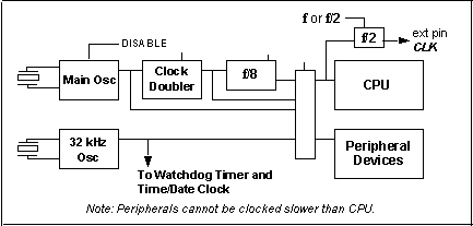
There are two crystal oscillators built into the Rabbit. The main oscillator accepts crystals up to a frequency of 29.4912 MHz (first overtone crystals only). The clock oscillator requires a 32.768 kHz crystal, which is powered by VBAT, and can be battery-backed.
An external oscillator or clock can be substituted for either crystal by connecting the external clock to XTALA1 or XTALB1 and leaving the other crystal pin (XTALA2 or XTALB2) unconnected. If an external oscillator is used for the main clock the output pin CLK (pin 1) should be used if the clock is needed externally. This signal is synchronized with the internal clock. In comparison, the internal clock is delayed by approximately 10 nanoseconds compared to the external oscillator input XTALB1.
The main oscillator is normally used to derive the clock for the processor and peripherals. The 32.768 kHz oscillator is normally used to clock the watchdog timer, the battery backable time/date clock, and the periodic interrupt. The main oscillator can be shut down in a special low-power mode of operation, and the 32.768 kHz oscillator is then used to clock all the things normally clocked by the main oscillator. This results in slower execution at low power (~200 µA).
The on-chip routing of the clocks is shown in Figure 7-1. The main oscillator can be doubled in frequency and/or divided by 8. If both doubling and dividing are enabled, then there will be a net division by 4. The CPU clock can optionally by divided by 2 and then optionally drive the external pin CLK. In many cases the clock is not needed externally, and in that case CLK can be used as a general-purpose output pin. The divide-by-2 option is available to minimize electromagnetic radiation if the is clock is driven off chip.
7.3 Clock Doubler
The clock doubler is provided to allow a lower frequency crystal to be used for the main oscillator and to provide an added range of clock frequency adjustability. The clock doubler is controlled via the Global Clock Double Register as shown in Table 7-2.
Table 7-3 lists the recommended values or "settings" for the Global Clock Double Register for various oscillator frequencies.
Table 7-3. Recommended Delays Set In GCDR for Clock Doubler Recommended GCDR Value Frequency Range
When the clock doubler is used and there is no subsequent division of the clock, the output clock will be asymmetric, as shown in Figure 7-2.
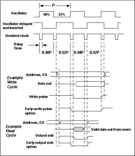
The doubled clock-low time is subject to wide (50%) variation since it depends on process parameters, temperature, and voltage. The times given above are for a supply voltage of 5 V and a temperature of 25°C. The doubled clock-low time increases by 20% when the voltage is reduced to 4 V, and increases by about 40% when the voltage is reduced further to 3.3 V. The values increase or decrease by 1% for each 5°C increase or decrease in temperature. The doubled clock is created by xor'ing the delayed and inverted clock with itself. If the original clock does not have a 50-50 duty cycle, then alternate clocks will have a slightly different length. Since the duty cycle of the built-in oscillator can be as asymmetric as 52-48, the clock generated by the clock doubler will exhibit up to a 4% variation in period on alternate clocks. This does not affect the no-wait states memory access time since two adjacent clocks are always used. However, the maximum allowed clock speed must be reduced by 10% if the clock is supplied via the clock doubler. The only signals clocked on the falling edge of the clock are the memory and I/O write pulses, and these have noncritical timing. Thus the length of the clock low time is noncritical as long as it is not so long as to shorten the clock high time excessively, which could make the write pulse too short for the memory used. This is unlikely to happen with practical clock speeds and typical static RAM memories.
The power consumption is proportional to the clock frequency, and for this reason power can be reduced by slowing the clock when less computing activity is taking place. The clock doubler provides a convenient method of temporarily speeding up or slowing down the clock as part of a power management scheme.
7.4 Controlling Power Consumption
The processor power consumption can be traded against speed by slowing the system clock, adding wait states, using low-power-consumption instructions, and for maximum power savings disabling the main system oscillator and using the real-time clock oscillator to provide the clock. The following power saving features can be enabled.
- Add memory wait states for instruction fetching. Total wait states are programmable as 0, 1, 2 or 4. Generally two wait states should use half the power of zero wait states.
- If the clock doubler is not already in use, divide both the processor and the peripheral clock by 4. This is permissible if nothing, particularly timers and serial ports, depends on the peripheral clock.
- If the clock doubler is in use, turn it off, dividing both processor and peripheral by 2.
- Divide the processor and/or peripheral clock by 8.
- Run code in RAM rather than flash memory.
- Switch the processor and peripheral clock to the 32.768 kHz oscillator and, if desired, disable the main oscillator.
- Execute a low-power instruction loop consisting mostly of instructions that don't use much power. The best choice is successive mul instructions that multiply 0 x 0. No intervening instructions are needed to load the terms to be multiplied after the first mul since all registers involved stay at zero.
It is anticipated that these measures would reduce current consumption to as low as 25 µA plus some leakage that would be significant at high operating temperatures.
7.5 Output Pins CLK, STATUS, /WDTOUT, /BUFEN
Certain output pins can have alternate assignments as specified in Table 7-4.
7.6 Time/Date Clock (Real-Time Clock)
The time/date clock (RTC) is a 48-bit (ripple) counter that is driven by the 32.768 kHz oscillator. The RTC is a modified ripple counter composed of six separate 8-bit counters. The carries are fed into all six 8-bit counters at the same time and then ripple for 8 bits. The time for this ripple to take place is a few nanoseconds per bit, and certainly should not should not exceed 200 ns for all 8 bits, even when operating at low voltage.
The 48 bits are enough bits to count up 272 years at the 32 kHz clock frequency. By convention, 12 AM on January 1, 1980, is taken as time zero. Rabbit Semiconductor software ignores the highest order bit, giving the counter a capacity of 136 years from January 1, 1980. To read the counter value, the value is first transferred to a 6-byte holding register. Then the individual bytes may be read from the holding registers. To perform the transfer, any data bits are written to RTC0R, the first holding register. The counter may then be read as six 8-bit bytes at RTC0R through RTC5R. The counter and the 32 kHz oscillator are powered from a separate power pin that can be provided with power while the remainder of the chip is powered down. This design makes battery backup possible. Since the processor operates on a different clock than the RTC, there is the possibility of performing a transfer to the holding registers while a carry is taking place, resulting in incorrect information. In order to prevent this, the processor should do the clock read twice and make sure that the value is the same in both reads.
If the processor is itself operating at 32 kHz, the read-clock procedure must be modified since a number of clock counts would take place in the time needed by the slow-clocked processor to read the clock. An appropriate modification would be to ignore the lower bytes and only read the upper 5 bytes, which are counted once every 256 clocks or every 1/128th of a second. If the read cannot be performed in this time, further low-order bits can be ignored.
The RTC registers cannot be set by a write operation, but they can be cleared and counted individually, or by subset. In this manner, any register or the entire 48-bit counter can be set to any value with no more than 256 steps. If the 32 kHz crystal is not installed and the input pin is grounded, no counting will take place and the six registers can be used as a small battery-backed memory. Normally this would not be very productive since the circuitry needed to provide the power switchover could also be used to battery-back a regular low-power static RAM.
7.7 Watchdog Timer
The watchdog timer is a 17-bit counter. In normal operation it is driven by the 32.768 kHz clock. When the watchdog timer reaches any of several values corresponding to a delay of from 0.25 to 2 seconds, it "times out." When it times out, it emits a 1-clock pulse from the watchdog output pin and it resets the processor via an internal circuit. To prevent this timeout, the program must "hit" the watchdog timer before it times out. The hit is accomplished by storing a code in WDTCR. Note that although a watchdog timeout resets the processor, it does not reset the timeout period stored in the WDTCR. This was done intentionally because an application may require the initialization of the processor resulting from the watchdog timeout to be based on a specific timeout period that is different from that of the reset initialization.
The watchdog timer may be disabled by storing a special code in the WDTTR register. Normally this should not be done unless an external watchdog device is used. The purpose of the watchdog is to unhang the processor from an endless loop caused by a software crash or a hardware upset.
It is important to use extreme care in writing software to hit the watchdog timer (or to turn off the watchdog timer). The programmer should not sprinkle instructions to hit the watchdog timer throughout his program because such instructions can become part of an endless loop if the program crashes and thus disable the recovery ability given by having a watchdog.
The following is a suggested method for hitting the watchdog. An array of bytes is set up in RAM. Each of these bytes is a virtual watchdog. To hit a virtual watchdog, a number is stored in a byte. Every virtual watchdog is counted down by an interrupt routine driven by a periodic interrupt. This can happen every 10 ms. If none of the virtual watchdogs has counted down to zero, the interrupt routine hits the hardware watchdog. If any have counted down to zero, the interrupt routine disables interrupts, and then enters an endless loop waiting for the reset. Hits of the virtual watchdogs are placed in the user's program at "must exercise" locations.
The code to do this may also hit the watchdog with a 0.25-second period to speed up the reset. Such watchdog code must be written so that it is highly unlikely that a crash will incorporate the code and continue to hit the watchdog in an endless loop. The following suggestions will help.
- Place a jump to self before the entry point of the watchdog hitting routines. This prevents entry other than by a direct call or jump to the routine.
- Before calling the routine, set a data byte to a special value and then check it in the routine to make sure the call came from the right caller. If not, go into an endless loop with interrupts disabled.
- Maintain data corruption flags and/or checksums. If these go wrong, go into an endless loop with interrupts off.
7.8 System Reset
The Rabbit has a master reset input (/RESET), which initializes everything in the device except for the RTC. This reset is delayed until the completion of any write cycles in progress to prevent any potential corruption of memory. If no write cycles are in progress, the reset takes effect immediately.
The purpose of inhibiting the completion of reset until write cycles in progress are completed is to protect variables in battery-backed memory from corruption when a reset takes place. However, if the power controller responsible for battery switchover blocks the chip select signal to the RAM, the writes in progress will be aborted in any case. This is not necessarily serious as software schemes can be used to protect critical variables in battery-backed memory.
The reset sequence requires a minimum of 128 cycles of the fast oscillator to complete, even if no write cycles were in progress at the start of the reset. Reset forces both the processor clock and the peripheral clock in the divide-by-eight mode. Note that if the processor is being clocked from the 32 kHz oscillator, the 128 cycles of the fast oscillator will probably not be sufficient to allow any writes in progress to be completed before the reset sequence completes and the clocks switch to divide-by-eight mode.
During reset, all of the memory control signals are held inactive. After the /RESET signal is inactive (high), the processor begins fetching instructions and the memory control signals begin normal operation. Note that the default values in the Memory Bank Control registers select four wait states per access, so the initial program fetch memory reads are 48 clock cycles long (8 x (2 + 4)). Software can immediately adjust the processor timing to whatever the system requires.
The default selection for the memory control signals consists of /CS0, /OE0 and /WE0, and writes are enabled. This selection can also be immediately programmed to match the hardware configuration. A typical sequence would be to speed up the clock to full speed, then select the appropriate number of wait states and the chip select signals, output enable signals and write enable signals. At this point software would usually check the system status to determine what type of reset just occurred and begin normal operation.
Table 7-10 describes the state of the I/O pins after an external reset is recognized by the Rabbit CPU. Note that the /RESET signal must be held low for three clocks for the processor to begin the reset sequence. There is no facility to tri-state output lines such as the address lines and the memory and I/O control lines.
Table 7-10. Rabbit 2000 Reset Sequence and State of I/O Pins Pin Name Direction /RESET Low1 Recognized by CPU Post-Reset2 CLK
XTALA1
XTALA2
XTALB1
XTALB2
A[19:0]
D[7:0]
/WDTOUT
STATUS
SMODE[1:0]
/CS0
/CS1
/CS2
/OE0
/OE1
/WE0
/WE1
/BUFEN
/IORD
/IOWR
PA[7:0]
PB[7:0]
PC[7:0]
PD[7:0]
PE[7:0]
1 A low is recognized internally by the processor after a reset
2 The default state of the I/O ports after the completion of the reset and initialization sequences
7.9 Rabbit Interrupt Structure
An interrupt causes a call to be executed, pushing the PC on the stack and starting to execute code at the interrupt vector address. The interrupt vector addresses have a fixed lower byte value for all interrupts. The upper byte is adjustable by setting the registers EIR and IIR for external and internal interrupts respectively. There are only two external interrupts generated by transitions on certain pins in parallel port E.
The interrupt vectors are shown in Table 7-11.
The interrupts differ from most Z80 or Z180 interrupts in that the 256-byte tables pointed to EIR and IIR contain the actual instructions beginning the interrupt routines rather than a 16-bit pointer to the routine. The interrupt vectors are spaced 16 bytes apart so that the entire code will fit in the table for very small interrupt routines.
Interrupts have priority 1, 2 or 3. The processor operates at priority 0, 1, 2 or 3. If an interrupt is being requested, and its priority is higher than the priority of the processor, the interrupt will take place after then next instruction. The interrupt automatically raises the processor's priority to its own priority. The old processor priority is pushed into the 4-position stack of priorities contained in the IP register. Multiple devices can be requesting interrupts at the same time. In each case there is a latch set in the device that requests the interrupt. If that latch is cleared before the interrupt is latched by the central interrupt logic, then the interrupt request is lost and no interrupt takes place. This is shown in Table 7-12. The priorities shown in this table apply only for interrupts of the same priority level and are only meaningful if two interrupts are requested at the same time. Most of the devices can be programmed to interrupt at priority level 1, 2 or 3.
Table 7-12. Interrupts--Priority and Action to Clear Requests Priority Interrupt Source Action Required to Clear the Interrupt Highest
External 1
Automatically by interrupt acknowledge.
External 0
Automatically by interrupt acknowledge.
Periodic (2 kHz)
Read GCSR.
Timer B
Read TBCSR1.
Timer A
Read TACSR.
Slave Port
Write SPSR.
Serial Port A
Rx: Read SADR or SAAR.
Tx: Write SADR, SAAR or SASR
Serial Port B
Rx: Read SBDR or SBAR.
Tx: Write SBDR, SBAR or SBSR
Serial Port C
Rx: Read SCDR or SCAR.
Tx: Write SCDR, SCAR or SCSR
Lowest
Serial Port D
Rx: Read SDDR or SDAR.
Tx: Write SDDR, SDAR or SDSR
1 If the compare registers (TBMxR and TBLxR) are not written within the ISR, the interrupt will will only be requested once.
In the case of the external interrupts the only action that will clear the interrupt request is for the interrupt to take place, which automatically clears the request. A special action must be taken in the interrupt service routine for the other interrupts.
7.9.1 External Interrupts
There are two external interrupts. Because of a problem in the original Rabbit design, only one of these interrupts is available for general use. The problem was corrected in revisions A-C of the Rabbit 2000. (Refer to Appendix B for further information to determine which version of the Rabbit 2000 chip you are using.) If you are working with an original Rabbit 2000 chip, see Technical Note 301, Rabbit 2000 Microprocessor Interrupt Problem.
External interrupts take place on a transition of the input. The pulse catchers are programmable separately to detect a rising, a falling, or both edges. The pairs of pulse catchers that are connected to the same interrupt should be programmed for the same type of edge detection. Each of the interrupt pins has its own catcher device to catch the edge transition and request the interrupt. The pulse needs to be present for a least three peripheral clocks to be detected.
When the interrupt takes place, both pulse catchers associated with that interrupt are automatically reset. If both edges are detected before the corresponding interrupt takes place, because the triggering edges occur nearly simultaneously or because the interrupts are inhibited by the processor priority, then there will be only one interrupt for the two edges detected. The interrupt service routine can read the interrupt pins via parallel port E and determine which lines experienced a transition, provided that the transitions are not too fast. Interrupts can also be generated by setting up the matching port E bit as an output and toggling the bit.
7.9.2 Interrupt Vectors: INT0 - EIR,0x00/INT1 - EIR,0x08
When it is desired to expand the number of interrupts for additional peripheral devices, the user should use the interrupt routine to dispatch interrupts to other virtual interrupt routines. Each additional interrupting device will have to signal the processor that it is requesting an interrupt. A separate signal line is needed for each device so that the processor can determine which devices are requesting an interrupt.
The following code shows how the interrupt service routines can be written.
; External interrupt Routine #1
int1:
    IPRES    ; restore system priority
    RET      ; return and ignore interrupt
;
; External interrupt Routine #0 (programmed priority could be 3)
int2:
    PUSH IP  ; save interrupt priority
    IPSET 1  ; set to priority really desired (1, 2, etc.)
; insert body of interrupt routine here
;
    POP IP   ; get back entry priority
    IPRES    ; restore interrupted routine's priority
    RET      ; return from interrupt
7.10 Bootstrap Operation
The device provides the option of bootstrap from any of three sources: from the Slave Port, from Serial Port A in clocked serial mode, or from Serial Port A in asynchronous mode. This is controlled by the state of the SMODE pins after reset. Bootstrap operation is disabled if (SMODE1, SMODE0) = (0, 0).
Bootstrap operation inhibits the normal fetch of code from memory, and instead substitutes the output of a small internal boot ROM for program fetches. This bootstrap program reads groups of three bytes from the selected peripheral device. The first byte is the most significant byte of a 16-bit address, followed by the least-significant byte of a 16-bit address, followed by a byte of data. The bootstrap program then writes the byte of data to the downloaded address and jumps back to the start of the bootstrap program. The most significant bit of the address is used to determine the destination for the byte of data. If this bit is zero, the byte is written to the memory location addressed by the downloaded address. If this bit is one, the byte is written to the internal peripheral addressed by the downloaded address. Note that all of the memory control signals continue to operate normally during bootstrap.
Execution of the bootstrap program automatically waits for data to become available from the selected peripheral, and each byte transferred automatically resets the watchdog timer. However, the watchdog timer still operates, and bytes must be transferred often enough to prevent the watchdog timer from timing out.
Bootstrap operation is terminated when the SMODE pins are set to zero. The SMODE pins are sampled just prior to fetching the first instruction of the bootstrap program. If the SMODE pins are zero, instructions are fetched from normal memory starting at address 0x0000. The Slave Port Control register allows the bootstrap operation to be terminated remotely. Writing a one to bit 7 of this register causes the bootstrap operation to terminate immediately. So the sequence 0x80, 0x24, and 0x80 will terminate bootstrap operation.
Bootstrap operation is not restricted to the time immediately after reset because the boot ROM is addressed by only the four least significant bits of the address. So any time that the address ends in four zeros, if the SMODE pins are non-zero and bit 7 of the SPCR is zero, the bootstrap program will begin execution. This allows in-line downloading from the selected bootstrap port. Upon completion of the bootstrap operation, either by returning the SMODE pins to zero or setting the bit in the SPCR, execution will continue from where it was interrupted for the bootstrap operation.
The Slave Port is selected for bootstrap operation when (SMODE1, SMODE0) = (0, 1). In this case the pins of Parallel Port A are used for a byte-wide data bus, and selected pins of Parallel Ports B and E are used for the Slave Port control signals. Only Slave Port Data Register 0 is used for bootstrap operation, and any writes to the other data registers will be ignored by the processor, and can actually interfere with the bootstrap operation by masking the Write Empty signal.
Serial Port A is selected for bootstrap operation as a clocked serial port when SMODE = 10. In this case bit 7 of Parallel Port C is used for the serial data and bit 1 of Parallel Port B is used for the serial clock. Note that the serial clock must be externally supplied for bootstrap operation. This precludes the use of a serial EEPROM for bootstrap operation.
Serial Port A is selected for bootstrap operation as an asynchronous serial port when SMODE = 11. In this case bit 7 of Parallel Port C is used for the serial data and the 32 kHz oscillator is used to provide the serial clock. A dedicated divide circuit allows the use of the 32 kHz signal to provide the timing reference for the 2400 bps asynchronous transfer. Only 2400 bps is supported for bootstrap operation, and the serial data must be eight bits for proper operation.
When the first phase of a bootstrap is performed using Serial Port A, the TXA signal is not needed since the bootstrap is a one-way communication. After the reset ends and the bootstrap mode begins, TXA will be low, reflecting its function as a parallel port output bit that is cleared by the reset. This may be interpreted as a break signal by some serial communication devices. TXA can be forced high by sending the triplet 0x80, 0x50, 0x40, which stores 0x40 in parallel port C. An alternate approach is to send the triplet 0x80, 0x55, 0x40, which will enable the TXA output from bit 6 of parallel port C by writing to the parallel port C function register (0x55).
NOTE Although the TXA signal is not needed during the first phase of the boot procedure, sending the "byte triplets," two-way communication is required once the cold loader has been loaded. The transfer rate in any bootstrap operation must not be too fast for the processor to execute the instruction stream. The Write Empty signal acts as an interlock when using the Slave Port for bootstrap operation, because the next byte should not be written to the Slave Port until the Write Empty signal is active. No such interlock exists for the clocked serial and asynchronous bootstrap operation. In these cases, remember that the processor clock starts out in divide-by-eight mode with four wait states, and limit the transfer rate accordingly. In asynchronous mode at 2400 bps it takes about 4 ms to send each character, so no problem is likely unless the system clock is extremely slow.
| Rabbit Semiconductor www.rabbit.com |