
User's Manual
|
|
| Rabbit 2000 Microprocessor User's Manual |
|
5. Pin Assignments and Functions
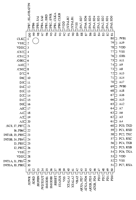
5.1 Package Schematic and Pinout
5.2 Package Mechanical Dimensions
Figure 5-2 shows the mechanical dimensions of the Rabbit PQFP package.
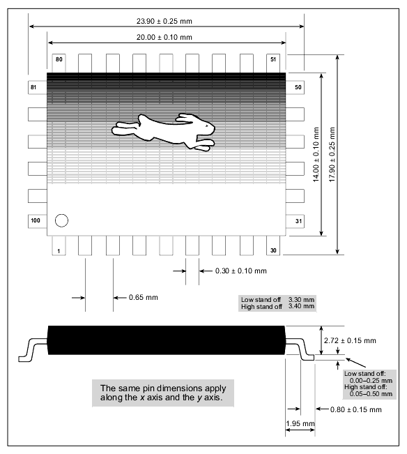
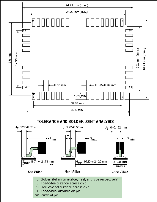
Figure 5-3 shows the PC board land pattern for the Rabbit 100-pin PQFP. This land pattern is RLP 711A, the registered land pattern for the Rabbit 2000 chip as developed by the Surface Mount Land Patterns Committee and specified in IPC-SM-782A, Surface Mount Design and Land Pattern Standard, IPC, Northbrook, IL, 1999.
5.3 Rabbit Pin Descriptions
Table 5-1 lists all the pins on the device, along with their direction, function, and pin number on the package.
Table 5-1. Rabbit Pin Descriptions Pin Group Pin Name Direction Function Pin Numbers Hardware
CLK
Output
Peripheral clock output. This signal is derived internally from the main system oscillator as perclk, and may be divided by 8, doubled, or both, by programmable internal circuitry. This signal is enabled after reset. Under program control, this pin can output the full internal clock frequency, or 1/2 the internal frequency, or it can be used as a general-purpose output pin under software control. See Table 7-4, "Global Output Control Register (GOCR = 0x0E)."
1
/RESET
Input
Master reset.
37
XTALA1
Input
Quartz crystal for 32 kHz clock oscillator. Lines to the crystal should be short and shielded from crosstalk. If an external clock is used, this pin should be driven by the external clock.
40
XTALA2
Output
Quartz crystal for 32 kHz crystal oscillator. Do not connect if an external clock is used.
41
XTALB1
Input
Quartz crystal for main system oscillator. Lines to the crystal should be short and shielded from crosstalk. If an external clock is used this pin should be driven by the external clock.
90
XTALB2
Output
Quartz crystal for main system oscillator. Do not connect if an external clock is used.
91
CPU Buses
A0-A19
Output
Address bus.
7, 17-20, 61-68, 70-75, 79
D0-D7
Bidirectional
Data bus.
9-16
Status/
Control
/WDTOUT
Output
WDT timeout--outputs a pulse when the internal watchdog times out. May also be used to output a 30 µs pulse.
34
Status
STATUS
Output
Programmable for functions:
1. driven low on first opcode fetch cycle
2. driven low during interrupt acknowledge cycle
3. to serve as a general-purpose output. See Table 7-4, "Global Output Control Register (GOCR = 0x0E).".
38
Status
SMODE1 SMODE0
Input
Startup mode select (SMODE1 = pin 35, SMODE0 = pin 36) to determine bootstrap procedure.
(SMODE1 = 0, SMODE0 = 0) start executing at address zero.
(0,1) cold boot from slave port.
(1,0) cold boot from clocked serial port A. (1,1) cold boot from asynchronous serial port A at 2400 bps.
The SMODE pins can be used as general input pins once the cold boot is complete.
35-36 (1:0)
Chip Selects
/CS0
Output
Memory Chip Select 0--connects directly to static memory chip select pin. Normally this pin is used to select base flash memory that holds the program.
8
/CS1
Output
Memory Chip Select 1--normally this pin is connected directly to static RAM chip select. /CS1 can be optionally forced continuously low under software control, a feature that aids in the use of battery-backed RAM when the chip select must pass through a controller that may have a slow propagation time.
5
/CS2
Output
Memory Chip Select 2--connect to static memory chip. Use this chip select last.
4
Output Enables
/OE0
Output
Memory Output Enable 0--connect directly to static memory chip.
6
/OE1
Output
Memory Output Enable 1--alternate memory output enable allows chip selects to be shared between two memory chips.
76
Write Enables
/WE0
Output
Memory Write Enable 0--connect directly to static memory chip. This pin may be disabled under software control to write protect the chip.
69
/WE1
Output
Memory Write Enable 1--connect directly to static memory chip. This pin may be disabled under software control to write protect the chip.
80
I/O Control
/BUFEN
Output
I/O Buffer Enable--this signal is driven low during an external I/O cycle and may be used to control 3-state enable on the bus buffer. The purpose is to save power by not driving the I/O address or data lines on every bus cycle.
33
I/O Read Strobe
/IORD
Output
I/O read strobe. Driven low on an external I/O read bus cycle. May be used to drive glue logic concerned with I/O expansion, such as the direction pin on a bidirectional bus buffer. See also programmable strobes in port E.
32
I/O Write Strobe
/IOWR
Output
I/O write strobe. Driven low as a write strobe during external I/O write cycles. Is enabled by the I/O bank control register. See also programmable strobes in port E.
31
I/O Port A
PA0-PA7
Input/
Output
These 8 bits serve as general-purpose input output or they serve as the data port for the slave port. On reset these pins are set to inputs and they float.
81-88
I/O Port B
PB0-PB7
6 In/2 Out
I/O Port B. When used as parallel I/O, PB7 and PB6 are outputs only. PB0-PB5 are inputs only.
PB0 and PB1 can be outputs when set up as the clock for the clocked serial ports. On reset, the outputs are set to zero. If the slave port is enabled, the following alternate assignments apply:
PB7--/SLAVEATTN: slave requests attention.
PB5, PB4--address lines (SA1, SA0) for slave registers.
PB3--slave negative read strobe from master.
PB2--slave negative write strobe from master.
If serial port A is enabled in clocked mode, then PB1 is the bidirectional clock line. If serial port B is enabled in clocked mode, then PB0 is the bidirectional clock line.
93-100
I/O Port C
PC0-PC7
4 In/4 Out
I/O Port C. When used as a parallel port, bits 1, 3, 5, 7 are inputs and bits 0, 2, 4, 6 are outputs. Bits 0, 2, 4, 6 can alternately be selectively enabled to serve as the serial data output for serial ports D, C, B, A respectively. Bits 1, 3, 5, 7 serve as the serial data inputs for serial ports D, C, B, A. These inputs can also be read from the parallel port register when they are being used by the serial port UART.
51, 54-60
I/O Port D
PD0-PD7
Input/
Output/
output open drain
I/O Port D. Each bit may be individually selected to be an input or output. Each output may be selected to be high-low drive or open drain. Outputs are buffered by timer-synchronizable registers for precision edge control. PD6 can be programmed to be an optional serial output for serial port A. PD4 can be programmed to be an optional serial output for serial port B. PD7 and PD5 can be used as alternate serial inputs by serial ports A and B, in which case these pins should be programmed as inputs.
43-50
I/O Port E
PE7-PE0
Input/
Output
I/O Port E. Each bit may be individually selected to be an input or output. Outputs are buffered by timer-synchronizable registers for precision edge control. Each of the port lines can be individually selected to be an I/O control signal instead of a parallel I/O line. Each of the 8 possible I/O control signals is a strobe energized on an external I/O cycle to 1/8th of the 64K external I/O space. Each strobe can be programmed to be a chip select, a write strobe, a read strobe or a combined read and write strobe. Any port bit used as an I/O control strobe must be programmed as an output bit. If the slave port is enabled, PE7 is used as the slave register chip select signal (negative active). PE7 should be programmed as an input for the slave register chip select function to work. If PE7 is programmed as an output and set low, then the slave register chip select will always be activated. PE0 and PE4 serve as alternate inputs for external interrupt 0. PE1 and PE5 serve as alternate inputs for external interrupt 1. If PE0 is enabled, then PE1 must also be enabled and similarly for PE4 and PE5. The interrupt is triggered in software on fall, rising or both edges. If both interrupts are enabled, they are or'ed together after edge detection has been performed on each input individually. The port bits must be set up as inputs for the to use them as interrupt request inputs.
21-26, 29, 30
Power
VBAT
+3.0 V (battery backup), +3.3 V or +5.0 V
42
VDD
+3.3 V or +5.0 V
3, 28, 53, 78, 92
VSS
Ground
2, 27, 39, 52, 77, 89
Serial Ports
CLKA
Input/
Output
Clock for serial port A when operating in synchronous mode. Alternate assignment for PB1.
94
CLKB
Input/
Output
Clock for serial port B when operating in synchronous mode. Alternate assignment for PB0.
93
RXA, TXA, RXB, TXB, RXC, TXC, RXD, TXD
RX--input
TX--output
Serial inputs and output for serial ports A-D. These are alternate pin assignments for parallel port C.
51, 54-60
ARXA, ATXA, ARXB, ATXB
RX--input
TX--output
Alternate serial inputs and output for serial ports A and B. These are alternate pin assignments for parallel port D, PD4-PD7.
43-46
Slave Port
SD0-SD7
Bidirectional
Slave port data bus. An alternate assignment for parallel port A.
81-88
/SLAVEATTN
Output
/SLAVEATTN--Slave is requesting attention from the master. An alternate pin assignment for parallel port B, bit 7.
100
/SRD
Input
Strobe used to read one of the slave registers. An alternate pin assignment for parallel port B, bit 3.
96
/SWR
Input
Strobe used to write a slave register. An alternate pin assignment for parallel port B, bit 2.
95
SA0, SA1
Input
Address lines to address slave registers. An alternate pin assignment for parallel port B, bits 4 and 5.
97,98
/SCS
Input
Chip select for slave port, active low. An alternate pin assignment for parallel port E, bit 7.
21
I/O Strobes
/I0,/I1,
/I2, /I3,
/I4, /I5,
/I6, /I7
Outputs
I/O strobes. Each strobe uses 1/8th of the I/O space or 8K addresses. Each strobe can be programmed as: chip select, read, write, combined read or write. These are alternate pin assignment for parallel port E, bits 0-7. Each pin may be individually re-assigned from parallel port to strobe functionality.
21-26, 29, 30
External Interrupt 0
INT0A, INT0B
Inputs
These pins are sampled and an interrupt request for external interrupt number 0 is latched on a specified transition (pos, neg, either). There is a separate latch for each pin. May be enabled when this pin is set up as input for parallel port E. The value of the pin may also be read via the parallel port. Uses bits 0, 4 of the parallel port. If parallel port is set up as output, the parallel port output may be used to cause the interrupt.
24, 30
External Interrupt 1
INT1A, INT1B
Inputs
These pins are sampled and an interrupt request for external interrupt number 1 is latched on a specified transition (pos, neg, either). There is a separate latch for each pin. May be enabled when this pin is set up as input for parallel port E. The value of the pin may also be read via the parallel port. Uses bits 1, 5 of the parallel port. If parallel port is set up as output, the parallel port output may be used to cause the interrupt.
23, 29
5.4 Bus Timing
The external bus has essentially the same timing for memory cycles or I/O cycles. A memory cycle begins with the chip select and the address lines. One clock later, the output enable is asserted for a read. The output data and the write enable are asserted for a write.
In some cases, the timing shown in Figure 5-4 may be prefixed by a false memory access during the first clock, which is followed by the access sequence shown in Figure 5-4. In this case, the address and often the chip select will change values after one clock and assume the final values for the memory to be actually accessed. Output enable and write enable are always delayed by one clock from the time the final, stable address and chip select are enabled. Normally the false memory access attempts to start another instruction access cycle, which is aborted after one clock when the processor realizes that a read data or write data bus cycle is needed. The user should not attempt a design that uses the chip select or a memory address as a clock or state changing signal without taking this into consideration.
5.5 Description of Pins with Alternate Functions
5.6 DC Characteristics
Table 5-3. Rabbit 2000 Absolute Maximum Ratings Symbol Parameter Maximum Rating Operating Temperature
Storage Temperature
Maximum Input Voltage1
Maximum Operating Voltage
Max Current Through Input Protection Diodes
1 The minimum voltage is -0.6 V DC, which may undershoot to -2.0 V for pulses that are shorter than 20 ns. The maximum output pin voltage is VDD + 0.75 V DC, which may overshoot for pulses that are shorter than 20 ns.
NOTE Stresses beyond those listed in Table 5-3 may cause permanent damage. The ratings are stress ratings only, and functional operation of the Rabbit 2000 chip at these or any other conditions beyond those indicated in this section is not implied. Exposure to the absolute maximum rating conditions for extended periods may affect the reliability of the Rabbit 2000 chip. 5.6.1 5.0 Volts
Table 5-4 outlines the DC characteristics for the Rabbit at 5.0 V over the recommended operating temperature range from Ta = -40°C to +85°C, VDD = 4.5 V to 5.5 V.
Table 5-4. 5.0 Volt DC Characteristics Symbol Parameter Test Conditions Min Typ Max Units IIH
Input Leakage High
VIN = VDD, VDD = 5.5 V
10
µA
IIL
Input Leakage Low
(no pull-up)
VIN = VSS, VDD = 5.5 V
-10
µA
IOZ
Output Leakage (no pull-up)
VIN = VDD or VSS,
VDD = 5.5 V
-10
10
µA
VIL
CMOS Input Low Voltage
0.3 x VDD
V
VIH
CMOS Input High Voltage
0.7 x VDD
V
VT
CMOS Switching Threshold
VDD = 5.0 V, 25°C
2.4
V
VOL
CMOS Output Low Voltage
IOL = See Table 5-6 (sinking)
VDD = 4.5 V
0.2
0.4
V
VOH
CMOS Output High Voltage
IOH = See Table 5-6 (sourcing)
VDD = 4.5 V
0.7 x VDD
4.2
V
5.6.2 3.3 Volts
Table 5-5 outlines the DC characteristics for the Rabbit at 3.3 V over the recommended operating temperature range from Ta = -40°C to +85°C, VDD = 2.7 V to 3.6 V.
Table 5-5. 3.3 Volt DC Characteristics Symbol Parameter Test Conditions Min Typ Max Unit s IIH
Input Leakage High
VIN=VDD, VDD=3.6V
5
µA
IIL
Input Leakage Low (no pull-up)
VIN=VSS, VDD=3.6V
-5
µA
IOZ
Output Leakage (no pull-up)
VIN=VDD or VSS, VDD=3.6V
-5
5
µA
VIL
CMOS Input Low Voltage
0.3 x VDD
V
VIH
CMOS Input High Voltage
0.7 x VDD
V
VT
CMOS Switching Threshold
VDD=3.0V, 25°C
1.5
V
VOL
CMOS Output Low Voltage
IOL= See Table 5-6 (sinking)
VDD=2.7V
0.11
0.4
V
VOH
CMOS Output High Voltage
IOH= See Table 5-6 (sourcing)
VDD=2.7V
0.7 x VDD
2.3
V
5.7 I/O Buffer Sourcing and Sinking Limit
Unless otherwise specified, the Rabbit I/O buffers are capable of sourcing and sinking 8 mA of current per pin at full AC switching speed. Full AC switching assumes 22.11 MHz CPU clock and capacitive loading on address and data lines of less than 100 pF per pin. Address pin A0 and Data pin D0 are rated at 16 mA each.
Table 5-6 shows the AC and DC output drive limits of the parallel I/O buffers.
Table 5-6. I/O Buffer Sourcing and Sinking Capability Pin Name Output Drive Sourcing1/Sinking2 Limits
(mA)Output Port Name
Full AC Switching
SRC/SNK
Maximum3 DC Output Drive
SRC/SNK
PA [7:0]
8/8
12/12
PB [7:6]
8/8
12/12
PC [6, 4, 2, 0]
8/8
12/12
PD [7:4]
8/8
12/12
PD [3:0]4
16/16
25/25
PE [7:0]
8/8
12/12
1 The maximum DC sourcing current for I/O buffers between VDD pins is 112 mA.
2 The maximum DC sinking current for I/O buffers between VSS pins is 150 mA.
3 The maximum DC output drive on I/O buffers must be adjusted to take into consideration the current demands made my AC switching outputs, capacitive loading on switching outputs, and switching voltage.
The current ascribed to AC switching is the average current that flows while AC switching is taking place. This can be computed using I = CVf, where f is the number of transitions per second, C is the capacitance switched, and V is the voltage swing. For example, if 12,000,000 transitions per second take place with a 5 V swing driving 100 pF, then I = 6 mA for one pin. The current attributable to all the pins between the power or ground pins must be summed to test the limits, including the current attributable to switching current or DC current.
The current drawn by all switching and non-switching I/O must not exceed the limits specified in the first two footnotes.
4 The combined sourcing from Port D [7:0] may need to be adjusted so as not to exceed the 112 mA sourcing limit requirement specified above.
| Rabbit Semiconductor www.rabbit.com |