|
|
| << Previous | Index | Next >> | |
| | |
Core designs can be developed around the Rabbit 2000 microprocessor. A core design includes memory, the microprocessor, oscillator crystals, the Rabbit standard programming port, and in some cases a power controller and power supply. Although modern designs usually use at least four-layer printed circuit boards, two-sided boards are a viable option with the Rabbit, especially if the clock speed is not high and the design is intended to operate at 2.5 V or 3.3 V--factors which reduce edge speed and electromagnetic radiation.
Schematics illustrating the use of the Rabbit microprocessor are available at www.rabbitsemiconductor.com.
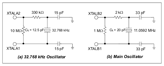
3.1 Clocks
The Rabbit has two built-in oscillators. The 32.768 kHz clock oscillator is needed for the battery-backable clock (aka, the real-time clock), the watchdog timer, and the cold boot function. The high frequency main oscillator is generally used to provide the main CPU clock.
The 32.768 kHz oscillator is slow to start oscillating after power-on. For this reason a wait loop in the BIOS waits until this oscillator is oscillating regularly before continuing the startup procedure. The startup delay may be as much as 5 seconds. Crystals with low series resistance (R < 35 kW) will start faster. If the clock is battery-backed, there will be no startup delay since the oscillator is already oscillating.
3.1.1 Low-Power Design
The power consumption is proportional to the clock frequency and to the square of the operating voltage. Thus, operating at 3.3 V instead of 5 V will reduce the power consumption by a factor of 10.9/25 or 43% of the power required at 5 V. The clock speed is reduced proportionally to the voltage at the lower operating voltage. Thus the clock speed at 3.3 V will be about 2/3 of the clock speed at 5 V. The operating current is reduced in proportion to operating voltage.
The Rabbit does not have a "standby" mode that some microprocessors have. Instead, the Rabbit has the ability to switch its clock to the 32.768 kHz oscillator. This is called the sleepy mode. When this is done, the power consumption is dramatically decreased. The current consumption is often reduced to the region of 100 µA at this clock speed. The Rabbit executes about 6 instructions per millisecond at this low clock speed. Generally, when the speed is reduced to this extent, the Rabbit will be in a tight polling loop looking for an event that will wake it up. The clock speed is increased to wake up the Rabbit.
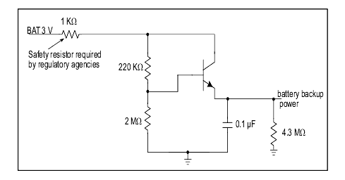
If current consumption by the real-time clock (RTC) is important, the regulator circuit shown in the figure below will reduce the current consumption by a substantial amount when a 3 V lithium battery is used. Using this circuit, the battery-backed clock requires less than 25 µA. If the full 3 V is used, the current consumption will be approximately 70 µA.
3.1.2 Conformal Coating of 32.768 kHz Oscillator Circuit
This circuit has low microampere level circuits. To avoid leakage due to moisture and ionic contamination it is recommended that the oscillator circuit be conformally coated. This is simplified if all components are kept on the same side of the board as the processor. Feedthroughs that pass through the board and are connected to the oscillator circuit should be covered with solder mask which will serve as a conformal coating for the back side of the board from the processor. An application note on conformal coating is available from Rabbit Semiconductor.
3.2 Basic Memory Design
Normally /CS0 and /OE0 and /WE0 should be connected to a flash memory that holds the startup code that executes at address zero. When the processor exits reset with (SMODE1, SMODE0) set to (0,0), it will attempt to start executing instructions at the start of the memory connected to /CS0, /OE0, and /WE0.
By convention, the basic RAM memory should be connected to /CS1, /OE1, and /WE1. /CS1 has a special property that makes it the preferred chip select for battery-backed RAM. A bit may be set in the MMIDR register to force /CS1 to stay enabled (low). This capability can be used to counter a problem encountered when the chip select line is passed through a device that is used to place the chip in standby by raising /CS1 when the power is switched over to battery backup. The battery switchover device typically has a propagation delay that may be 20 ns or more. This is enough to require the insertion of wait states for RAM access in some cases. By forcing /CS1 low, the propagation delay is not a factor because the RAM will be always selected and will be controlled by /OE1 and /WE1. If this is done, the RAM will consume more power while not battery-backed than it would if it were run with dynamic chip select and a wait state. If this special feature is used to speed up access time for battery backed RAM then no other memory chips should be connected to /OE1 and /WE1.
3.2.1 Memory Access Time
The memory access time required depends on the clock speed and the capacitive loading of the address and data lines. Wait states can be specified by programming to accommodate slow memories for a given clock speed. Wait states should be avoided with memory that holds programs because there is a significant slowing of the execution speed. Wait states are far more important in the instruction memory than in the data memory since the great majority of accesses are instruction fetches. Going from 0 to 1 wait states is about the same as reducing the clock speed by 30%. Going from 0 to 2 wait states is worth approximately a 45% reduction in clock speed. A table of memory access times required for various clock speeds is given in the Rabbit 2000 Microprocessor User's Manual.
3.2.2 Precautions for Unprogrammed Flash Memory
If a Rabbit-based system is powered up and released from reset when not in one of the cold boot modes, the processor attempts to begin execution by reading from address zero of the memory attached to /CS0, /OE0, and /WE0. If this memory is an unprogrammed or improperly programmed flash memory, there is a danger that the memory could be destroyed if the write security feature of the flash memory is disabled. Flash memories have a write security feature that inhibits starting write cycles unless a special code is first stored to the memory. For example, Atmel flash memories use the bytes AAh, 55h, and A0h stored to addresses AAAAh or 5555h in a particular sequence. Any write executed that is not prefixed by this sequence will be ignored. If the memory has write protection disabled, and execution starts, it is possible that an endless loop that includes a write to memory will establish itself. Since the flash memory wears out after a few hundred thousand writes, the memory could be damaged in a short period of time by such a loop. Unfortunately, flash memory is shipped from the factory with the protection feature disabled to accommodate obsolete memory programmers.
The solution to this problem is to order the memory with the write protection enabled, or to enable it with a flash programming system. Then the memory will be safe if it is soldered into the Rabbit system. If an unsafe memory is soldered into a system, then the memory can be powered up with the programming cable connected, and a sequence can be sent using the cold boot procedure to enable the write protection. Compiling any Dynamic C program to the flash will make the memory safe. If this is not convenient, tester software can make the memory safe by sending a byte sequence over the programming connection serial link.
The following example shows a program that can be downloaded via the cold boot protocol to make a Atmel AT29C010A 128K x 8 flash memory safe. In this case, the RAM connected to /CS1 is used to hold a program starting at address zero. The flash memory is mapped into the data segment starting at address 1000h for access to the start of the flash memory.
; Before storing this program, the RAM is mapped to the first quadrant.
; The program resides at address zero in RAM.
; NOTE: this program has not been testedld a,0e1h ; 3e e1 segsize reg
ioi ld (13h),a ; d3 32 13 00 data seg starts at 1000h
ld a,3fh ; 3e 3f dataseg reg
ioi ld(12h),a ; d3 32 12 00 set data seg base of flash to 1000h
ld a,0 ; 3e 00 for MB1CR memory bank reg for flash on CS0
ld (15h),a ; 32 15 00 bank 1 reads flash starting at 256k
ld a,0aah ; 3e aa
ld (5555h+1000h),a ; 32 55 65 first byte of unlock code
ld a,55h ; 3e 55
ld (2AAAh+1000h),a ; 32 aa 3a 2nd byte of unlock code
ld a,0a0h ; 3e a0
ld (5555h+1000h),a ; 32 55 65 3rd byte of unlock code
ld hl,1000h ; 21 00 10 point to start of flash memory
ld (hl),0c3h ; 36 c3 jump op code
inc hl ; 23
ld (hl),00h ; 36 00 zero
inc hl ; 23
ld (hl),00h ; 36 00 zero
jr * ; 18 fe end with endless loopThis code can be sent by means of a sequence of triplets via the serial port.
80 14 01             ; I/O write 01 to 0000 MB0CR select cs1- map RAM to Q1
00 00 3e             ; write to memory address 0
00 01 e1
00 02 d3
00 03 32
00 04 12
00 05 00
; continue code above here
00 2b 18             ; last instruction
00 2c fe             ; last byte
80 24 80             ; start execution of program at zero
The program will execute within about 10 ms.
3.3 PC Board Layout and Memory Line Permutation
To use the PC board real estate efficiently, it is recommended that the address and data lines to memory be permuted to minimize the use of PC board resources. By permuting the lines, the need to have lines cross over each other on the PC board is reduced, saving feed-through's and space.
For static RAM, address and data lines can be permuted freely, meaning that the address lines from the processor can be connected in any order to the address lines of the RAM, and the same applies for the data lines. For example, if the RAM has 15 address lines and 8 data lines, it makes no difference if A15 from the processor connects to A8 on the RAM and vice versa. Similarly D8 on the processor could connect to D3 on the RAM. The only restriction is that all 8 processor data lines must connect to the 8 RAM data lines. If several different types of RAM can be accommodated in the same PC board footprint, then the upper address lines that are unused if a smaller RAM is installed must be kept in order. For example, if the same footprint can accept either a 128K x 8 RAM with 17 address lines or a 512K x 8 RAM with 19 address lines, then address lines A18 and A19 can be interchanged with each other, but not exchanged with A0-A17.
Permuting lines does make a difference with flash memory. If the memory is socketed and it is intended to program the memory off the board, then it is probably best to keep the address and data lines in their natural order. However, since the flash can be programmed in the circuit using the Rabbit programming port, it is expected that most designers will solder the flash memory directly to the board in an unprogrammed state. In this case, the permeation of data and address lines must still be taken into account because flash memory requires the use of a special unlock code that removes write protection. The unlock operation involves a special sequence of reads and writes accessing special addresses and writing the unlock codes.
Another consideration is that the flash memory may be divided into sectors. An entire sector must be written to modify the memory. Small-sector memories are divided into 1024 sectors. If the largest flash memory that is usable in a particular design is 512K, the largest sector size is 512 bytes. If the smallest memory used is 128K, then the smallest sector is 128 bytes. In order that the sector can be contiguous for all possible types of memory, the lower 7 address lines (A0...A6) should be permuted as a group. Address lines A7 and A8 should not be permuted at all if it is desirable to keep the larger sectors contiguous. The upper 10 address lines can be permuted as a separate group. The special memory chip addresses 05555h and 0AAAAh must be accessed as part of the unlock sequence. These addresses use only the first 16 address lines and have the odd and even numbered bits the same. The unlock codes use the numbers 55h, AAh or A0h.
Permuting data or address lines with flash memory should probably be avoided in practical systems.
3.4 PC Board Layout and Electromagnetic Interference
Most design failures are related to the layout of the printed circuit board (PCB). A good layout results when the effects of electromagnetic interference (EMI) are considered. EMI refers to unintentional radiation from the circuit board that might cause interference with other devices, mainly television sets. If the PCB layout meets EMI regulations, it will probably be otherwise electrically sound.
3.4.1 EMI Regulations
The Federal Communications Commission (FCC) regulates EMI standards in the United States. Their jurisdiction is all 50 states, the District of Columbia, and U.S. possessions. The European Union (EU) regulates EMI standards in Europe by means of a CE Marking that acts as a product's passport in the European market. The actual CE Marking is the letters "CE," an abbreviation of a French phrase "Conformite Europeene."
These regulations specify the maximum radiation measured in units of field strength (microvolts / meter) at a standard distance, usually 3 meters. The field strength must be measured using a particular type of filter (120 kHz wide) and a particular type of peak detection (quasi-peak). With Rabbit-based systems, the radiation will generally be pure tones at harmonics of the clock speed. This makes it unnecessary to use a special filter or quasi peak detection except for final verification measurements.
3.4.1.1 EMI Measuring Devices
The measurements are performed using a spectrum analyzer coupled to a calibrated antenna. The equipment needed to perform these tests may cost $25,000 or more. Many designers will use outside laboratories to perform the tests. There is not necessarily a legal requirement to perform the tests. It depends on the type of equipment and its intended use. For example, FCC regulations in the USA exempt industrial equipment.
3.4.1.2 Classes For EMI Testing
FCC computer regulations divide equipment into two classes.
Note that for field strength, 20 dB is a factor of 10 and 6 dB is a factor of 2. Field strength declines inversely with distance, so at 10 meters the field strength for the same device will be about 3/10ths as large as at 3 meters which is approximately 10 dB less. (20 dB is a factor of 10, 10 dB is a factor of the square root of 10 or 1/3.16 = 3.16/10.) These limits apply in the range of 30-230 MHz for the more restrictive CE test. Above 230 MHz the limit is 7 dB higher. Although the test range goes to 1 GHz, with Rabbit-based systems there will rarely be any concern above 300 MHz.
With a Rabbit-based system it is easy to meet the Class B limits if proper PCB layout precautions are observed. At Rabbit Semiconductor, our target is to beat the Class B limit by 10 dB.
3.4.2 Layout and Decoupling for Low EMI
Generally you should design with a 4 (or more) layer printed circuit board. The cost of a 4-layer board as compared to a 2-layer board is about 30% more per square inch and generally well worth it. Although we have not attempted it, a 2-layer design would probably work for lower clock frequencies if the ground and power nets are well gridded for power distribution (see Section 3.4.2.5 on page 18).
Usually a 4-layer printed circuit board has a ground plane and a power plane located as the two inner layers and connect layers on the top and bottom layers. Components may be mounted on only one side or on both sides. A 6-layer board places the ground and power layers as the middle two layers and then has two routing layers both above and below. Adjacent routing layers run traces at right angles to minimize coupling between signal traces. Sometimes the ground and power layers are placed on the outside of the boards, but this makes debugging more difficult and compromises the layers more since they have to be cut up for the component footprints.
3.4.2.1 EMI Sources
Most EMI comes from signals that are strictly regular. The main sources are the crystal oscillator, the lines emanating from the Rabbit chip that are affected by the internal clocking of the chip, and the actual clock or clock/2 if it is run around the printed circuit board. Address and data lines generate less EMI because there is no regular frequency on these lines since the bus cycles vary in length, shifting the signal phase constantly. A0 is the hottest address line since it is varying most rapidly and also has a stronger drive than the other address lines.
A square wave has harmonics at odd frequencies that decline in amplitude proportional to 1/f. A small wire that acts as an antenna radiates more the higher the frequency of excitation. The effectiveness as an antenna increases proportional to frequency. These two effects approximately cancel, resulting in an approximately flat spectrum for a typical printed circuit board. For example, without taking precautions, it would not be unusual to have a problem with the 7th harmonic, or 154.7 MHz when the Rabbit clock is 22.1 MHz. Above approximately 300 MHz, the edges are not fast enough to generate strong harmonics for typical Rabbit systems.
3.4.2.2 Clock Signal Pin 1
Pin 1 of the Rabbit can be programmed to output the internal clock or the internal clock divided by 2. The Rabbit BIOS automatically disables this pin, starting with Dynamic C 7.01. To minimize EMI, avoid using this pin as a clock output. Most Rabbit designs do not need to explicitly use the clock output pin. However, in cases that require a clock, use clock/2 if possible. Also, a series resistor can (and should) be placed in the clock line to slow down the rise and fall times, which will reduce radiation at higher harmonics of the frequency. Place the resistor, which might be around 1 K ohms, as close to pin 1 as possible. The capacitive load of whatever the clock line is connected to, along with the resistor, creates an RC time constant that slows the edge. If the capacitive load is larger, a smaller resistor is needed and vice versa.
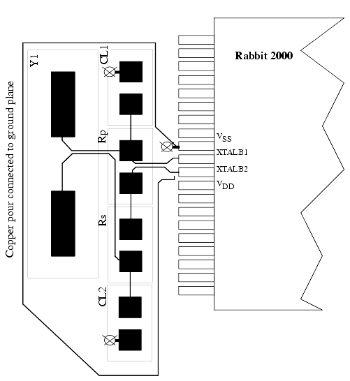
The clock line should be kept as short as possible, and run over a ground plane--or even better between two ground planes. It should be positioned well away from other traces, especially traces running parallel to it for any distance. Coupling to a parallel trace is greater the faster the edges. If you run parallel ground traces or a ground trace above the clock line then the parallel ground traces should be connected with very low inductance connections to the ground plane. This is done by using many feedthroughs.
Figure 3-3. Many feedthroughs provide very low inductance connections between parallel ground traces and a ground plane 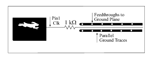
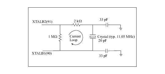
3.4.2.3 High Frequency Oscillator Circuit
The Rabbit's oscillator circuit typically runs at 11.05 MHz for a 22.1 MHz internal clock. The internal clock doubler is used to double the clock frequency. If the clock doubler is not used then the external oscillator circuit runs at the full internal clock frequency, resulting in more radiation from the external circuit due to its higher frequency. In either case there should not be excessive radiation from this circuit if layout guidelines are followed.
The main objective is to keep the loop area of the circuit small so as to avoid coupling the clock to other lines and because current circulating in a loop acts as an antenna. The part of the circuit most susceptible to radiation is the trace from pin 91 to the 2 kW resistor (see Figure below). The remainder of the circuit has the edges slowed by the 2 kW resistor.
The low frequency of the 32.768 kHz clock causes no radiation.
3.4.2.4 Processor Decoupling
The internal clock of the processor is routed throughout the silicon die. On the rising edge of the clock all the flip flops on the die are clocked within a nanosecond or so of each other, resulting in large current flows through the ground and power pins. The current surge is mainly due to the capacitance driven by the clock and by flip flops changing their state on the clock. The connections from the ground and power pins to the die have inductance, as do the connections within the die. The ground and power on the die will bounce up and down at the clock frequency and this will be coupled to all the other I/O lines that are clamped to power or ground by transistors. To minimize this bouncing a low impedance path from the pairs of ground and power pins to decoupling capacitors should be provided.
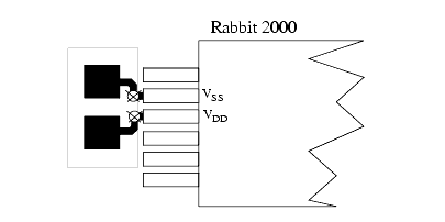
The Rabbit has 6 power and 6 ground pins. Of the six power pins, five reside on the main power grid and are used to power the CPU, peripherals and the I/O. The other one, pin 42, resides on a separate power net to supply the battery-backed clock. The ground pins are all tied to the common ground network.
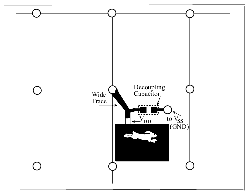
To minimize EMI, connect all power pins as directly as possible to a ground plane running under the processor without large slots or non-metal areas in the plane. A low inductance connection is obtained by a short and wide trace leading to the feedthrough to the ground plane. A pair of feedthroughs has less inductance than a single feedthrough. The power pins should be connected by a low inductance path to the power plane, or if there is no power plane, to a decoupling capacitor.
For capacitors immediately adjacent to the processor, use 10 nF decoupling capacitors (.01 µF). Larger capacitors have too much inductance, resulting in excessive harmonics above 100 MHz.
Decoupling of pin 42 (Vbat) is not critical since relatively small currents flow through this pin.
3.4.2.5 Elimination of Power Plane
If the power plane is eliminated or extensively slotted to accommodate routed traces, decoupling and power distribution becomes more critical. The key is to maintain a low inductance connection from "hot" package power pins to a decoupling capacitor. Also, keep the inductance between widely separated parts of the power net as low as possible. Gridding the net in a cross connect pattern will lower inductance between points, as will wider traces. The procedure is to use a grid and then use wide traces from grid intersections to the decoupling capacitors or packages.
| Rabbit 2000 Designer's Handbook |
<< Previous | Index | Next>> | rabbit.com |